What is DipTrace?
DipTrace is a powerful PCB design software package for creating printed circuit boards. It offers schematic capture, PCB layout, auto-routing, and Gerber export capabilities in an intuitive interface.
Some key features of DipTrace include:
- Schematic and PCB layout editors
- 3D board preview
- Real-time design rule checking (DRC)
- Autorouter and manual routing options
- Gerber files export
- 3D STEP model export
- Mechanical CAD export
- Multi-sheet and hierarchical schematic support
- High-speed design capabilities
DipTrace aims to make the PCB design process efficient for engineers, whether working on simple 2-layer boards or complex multi-layer high-density interconnect (HDI) PCBs. Its reasonable pricing also makes it an attractive option compared to some other PCB design software.
Getting Started with DipTrace
To start using DipTrace for your PCB projects, first download and install the software from the official DipTrace website. DipTrace offers a free version for non-commercial use as well as paid standard and advanced versions with additional features.
Upon launching DipTrace, you are presented with the main project manager window:
From here, you can create a new project, open an existing project, access component and pattern libraries, and launch the various editors within the DipTrace suite (schematic, PCB layout, pattern, component, etc.).
Creating a New Project
To create a new PCB project, click the “New Project” button in the project manager window. Give your project a name and specify the location to save project files. This creates a new blank project ready for designing your schematic.
The Schematic Editor
Double-click your new project in the project tree to open the schematic editor. The schematic editor is where you define the electrical connectivity of your PCB by placing component symbols and wiring them together.
The main parts of the schematic editor window are:
- Main menu – Access commands and tools
- Top toolbar – Frequently used tools and options
- Right toolbar – Component placement and editing tools
- Libraries panel – Browse available component libraries
- Design manager panel – Navigate schematic sheets and preview PCB
- Properties panel – View and edit properties of selected objects
- Messages panel – Displays electrical rule check (ERC) messages
To start your schematic design:
- Select desired components from the libraries panel and place them on the schematic sheet
- Use the wire tool to connect pins
- Add net labels, power and ground symbols as needed
- Create new schematic sheets for hierarchical designs
- Run ERC checks to verify correct connectivity

PCB Layout in DipTrace
Once your schematic is complete, you can convert it into a PCB layout to design the physical board. To convert the schematic to PCB:
- Click “Convert to PCB” in the top toolbar of the schematic editor
- Specify board origin coordinates and select which layers to import
- Click OK to create the PCB file and open the PCB layout editor
The PCB layout editor has a similar user interface to the schematic editor with some key differences:
- The main workspace shows the physical board shape and components
- The layer stackup and selection is in the right toolbar
- The left toolbar has shape drawing and placement tools
- The Design Manager panel shows footprints on the board instead of schematic sheets
Important steps to complete your PCB layout:
- Define the board shape using drawing tools
- Arrange components on the board
- Route connections between components either manually or with the autorouter
- Add copper fills for power planes and EMI shielding
- Include mounting holes, silkscreen, and any other mechanical details
- Run a Design Rule Check (DRC) to verify the layout meets manufacturing specs
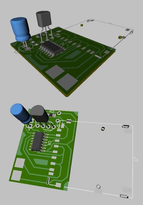
DipTrace includes a 3D viewer for previewing your PCB design as a realistic 3D model. This helps check mechanical clearances and visualize the final assembled board.

Gerber Files Export
After finalizing your PCB layout, you need to generate manufacturing files to have the board physically produced. The standard file formats for PCB fabrication are Gerber (RS-274X) and NC drill (Excellon) files.
Gerber files are a vector image format that represent copper layers, solder mask, silkscreen, and other board features. NC drill files are plain text files that specify the location and size of drilled holes.
DipTrace can easily export a complete set of Gerber and NC drill files for your PCB design. To generate manufacturing files:
- Go to File > Export > Gerber in the PCB layout editor
- The CAM export window will open showing available export options:
- Select the layers to export as Gerber files (copper, solder mask, paste, silkscreen)
- Choose the appropriate drill file format under NC Drill settings
- Specify any other needed options like coordinate format or aperture table
- Click Export and save the files in a new folder for your manufacturer
DipTrace will generate a zip package containing all the selected Gerber and drill files ready to send off for fabrication.
Gerber File Extensions
The generated Gerber files will have standard file extensions to indicate their layer type:
| Extension | Layer Type |
|---|---|
| .GTL | Top (outer) copper layer |
| .GBL | Bottom copper layer |
| .G1 | Inner copper layer 1 |
| .G2 | Inner copper layer 2 |
| … | … |
| .GTO | Top silkscreen overlay |
| .GBO | Bottom silkscreen |
| .GTP | Top solder paste (stencil) |
| .GBP | Bottom solder paste |
| .GTS | Top solder mask |
| .GBS | Bottom solder mask |
| .GM1 | Mechanical layer 1 |
| .GKO | Keep-out layer |
| .GPT | Top pad master |
| .GPB | Bottom pad master |
| .TXT | Drill / profile / rout info |
The NC drill files will have extensions .DRL (NC Drill) or .TXT (Excellon).
Always carefully review the generated files in a Gerber viewer to check for any errors or missing information before submitting them for manufacturing.

Frequently Asked Questions
What is the difference between Gerber RS-274D and RS-274X formats?
RS-274D, also known as Standard Gerber, is an older Gerber file format with some limitations. It lacks information about apertures and layer polarity. RS-274X or Extended Gerber is the newer format that includes aperture definitions, clear layer polarity, and support for embedded attributes. Always use RS-274X when possible for more complete and unambiguous data.
How do I check my exported Gerber files?
You can view Gerber files in a free Gerber viewer program to verify their contents before manufacturing. Some popular viewers are:
- GC-Prevue
- ViewMate
- Ucamco UcamX Free Gerber Viewer
- ZofzPCB
- Gerbv
Check the copper layers, drill layers, solder mask, and silkscreen for any obvious mistakes. Many online PCB manufacturers also offer free Gerber viewing and analysis tools when you upload your files for quoting.
What else do I need to provide to my PCB manufacturer?
In addition to the complete Gerber and NC drill files, you should generate a centroid or XY file that lists the coordinates and rotation of all SMT components on the board. This “pick and place” file is used to program assembly machines.
Some other helpful files to include:
- Bill of Materials (BOM) with manufacturer part numbers
- Any design notes, assembly drawings, or special instructions
- 3D STEP model for mechanical verification
- Solder paste stencil Gerber if you want a stencil for assembly
Can I export my PCB in other CAD formats?
Yes, in addition to Gerber files, DipTrace supports exporting in several other formats used for mechanical and 3D CAD. Available export options include:
- IDF (Intermediate Data Format) – ASCII PCB/mechanical interchange format
- DXF (Drawing Interchange Format) – 2D vector graphics and 3D model format
- STEP (Standard for the Exchange of Product Data) – 3D object exchange format
- Hyperlynx – Signal integrity simulation model format
- ODB++ (Open Database) – Intelligent CAD/CAM data exchange format
- IGES (Initial Graphics Exchange Specification) – 3D model format
These other export formats are useful for integrating your PCB design into mechanical designs, enclosures, and simulators. The standard Gerber RS-274X and Excellon NC drill formats remain the primary files needed for basic PCB fabrication.
Where can I learn more about using DipTrace?
DipTrace offers an extensive set of video tutorials, user guides, and a knowledgebase on their website: DipTrace Tutorials and User Guides
The user forum also has a wealth of information from other DipTrace users: DipTrace User Forum
Finally, many electronics engineering blogs and online course platforms have beginner tutorials and more advanced DipTrace tips. Some good resources:
- Getting Started with DipTrace
- KiCad Like a Pro (DipTrace tutorials)
- PCB Design Tutorial with DipTrace
With some practice and the help of these resources, you’ll be designing professional-quality PCBs in DipTrace and generating Gerber files with ease.


Leave a Reply