Understanding PCB Tolerance and Its Importance
Printed Circuit Board (PCB) tolerance is a critical aspect of PCB design and manufacturing, especially when dealing with miniature components like 0201 and Micro Ball Grid Array (BGA) packages. PCB tolerance refers to the acceptable deviation from the ideal dimensions and placement of various features on a PCB, such as traces, pads, and holes. Maintaining tight tolerances is essential for ensuring proper functionality, reliability, and compatibility of the PCB assembly.
In this article, we will delve into the world of PCB tolerance, focusing on 0201 and Micro BGA packages. We will discuss the challenges associated with these miniature components, the factors affecting PCB tolerance, and the best practices for designing and manufacturing high-quality PCBs with tight tolerances.
The Challenge of Miniaturization
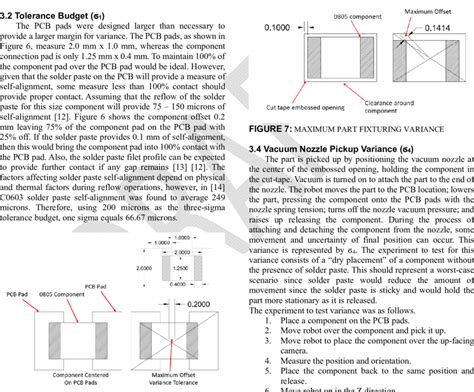
As electronic devices continue to shrink in size and increase in functionality, the demand for smaller components and higher component density on PCBs has grown tremendously. The 0201 package, measuring just 0.6mm x 0.3mm, and Micro BGA packages, with ball pitches as small as 0.3mm, have become increasingly popular in applications such as smartphones, wearables, and IoT devices.
However, working with these miniature components poses several challenges for PCB designers and manufacturers:
- Reduced feature sizes: Smaller components require narrower traces, smaller pads, and tighter clearances, pushing the limits of PCB fabrication capabilities.
- Increased precision requirements: The placement and alignment of miniature components demand higher precision to ensure proper connections and avoid short circuits or open connections.
- Enhanced thermal management: Higher component density leads to increased heat generation, requiring efficient thermal management strategies to prevent overheating and ensure reliability.
Factors Affecting PCB Tolerance
Several factors contribute to the overall tolerance of a PCB, including:
- Material selection: The choice of PCB substrate material, such as FR-4, Rogers, or polyimide, can impact the dimensional stability and thermal expansion of the board.
- Fabrication process: The accuracy and consistency of the PCB fabrication process, including etching, drilling, and plating, directly influence the achievable tolerances.
- Layer count: As the number of layers in a PCB increases, the challenges in maintaining tight tolerances also increase due to the accumulation of errors across multiple layers.
- Copper thickness: The thickness of the copper traces and pads can affect the etching process and the resulting feature sizes and tolerances.
- Environmental factors: Temperature, humidity, and other environmental conditions can cause PCBs to expand or contract, affecting the dimensional stability and tolerance of the board.
Designing for Tight Tolerances
To successfully design PCBs with 0201 and Micro BGA components, engineers must follow best practices and consider several key factors:
1. Design Rules and Guidelines
Adhering to the recommended design rules and guidelines provided by the PCB manufacturer and component suppliers is crucial. These rules specify the minimum feature sizes, clearances, and spacing requirements for various aspects of the PCB design, such as:
- Trace width and spacing
- Pad size and shape
- Solder mask opening
- Drill hole size and location
- Silkscreen markings
By following these guidelines, designers can ensure that their PCBs are manufacturable and meet the required tolerances.
2. CAD Tools and DFM Analysis
Using advanced Computer-Aided Design (CAD) tools with built-in Design for Manufacturability (DFM) analysis capabilities can help designers identify and resolve potential issues related to PCB tolerance. These tools can check the design against the specified manufacturing constraints and provide feedback on areas that may require adjustments to improve manufacturability and minimize tolerance issues.
3. Component Placement and Orientation
Careful consideration of component placement and orientation is essential for maintaining tight tolerances. Designers should:
- Place components in a way that minimizes the risk of tombstoning (when a component stands up on one end during reflow soldering) or skewing.
- Orient components to facilitate easier assembly and minimize the chances of misalignment.
- Provide adequate clearances between components to allow for proper solder joint formation and avoid short circuits.
4. Panelization and Breakout Tabs
When designing PCBs with tight tolerances, it is important to consider the panelization process and the use of breakout tabs. Panelization involves grouping multiple PCBs onto a single panel for efficient fabrication and assembly. Breakout tabs are small sections of the PCB that connect individual boards to the main panel, allowing for easy separation after assembly.
Designers should work closely with the PCB manufacturer to determine the optimal panelization layout and breakout tab design to minimize stress on the individual boards and ensure accurate registration during the fabrication and assembly processes.
Manufacturing Considerations
Achieving tight tolerances in PCB manufacturing requires a combination of advanced equipment, skilled operators, and robust quality control processes.
1. Equipment and Process Control
PCB manufacturers must invest in high-precision equipment and maintain strict process control to consistently produce boards with tight tolerances. This includes:
- High-resolution imaging systems for accurate patterning of fine features
- Laser drilling machines for precise hole placement
- Automated optical inspection (AOI) systems for detecting defects and dimensional variations
- Real-time monitoring and control of critical process parameters, such as temperature, pressure, and chemical concentrations
2. Material Handling and Storage
Proper handling and storage of PCB materials, such as substrates, copper foils, and solder masks, are essential for maintaining their dimensional stability and minimizing the impact of environmental factors on the final board tolerance. Manufacturers should follow the material suppliers’ recommendations for storage conditions, shelf life, and handling procedures to ensure consistent results.
3. Quality Control and Inspection
Implementing a comprehensive quality control and inspection program is crucial for identifying and correcting tolerance issues during the manufacturing process. This includes:
- Incoming material inspection to verify the quality and consistency of raw materials
- In-process inspection at critical stages of fabrication to catch and correct any deviations from the specified tolerances
- Final inspection and testing to ensure that the finished PCBs meet all the required specifications and performance criteria

Case Studies and Examples
To better understand the challenges and solutions related to PCB tolerance in real-world applications, let’s look at a few case studies and examples.
Case Study 1: Smartphone Motherboard
A smartphone manufacturer was facing yield issues due to the tight tolerances required for the placement of a Micro BGA processor on the device’s motherboard. The initial design had a pad size of 0.25mm and a pitch of 0.5mm, which resulted in frequent misalignment and open connections during the assembly process.
To solve this issue, the PCB design team collaborated with the manufacturer to optimize the pad size and pitch. By increasing the pad size to 0.3mm and the pitch to 0.6mm, they were able to improve the assembly yield while still maintaining the required component density. Additionally, they implemented a more precise solder paste printing process and used a higher-resolution inspection system to detect any alignment issues early in the assembly process.
Case Study 2: Wearable Device Sensor Board
A wearable device manufacturer needed to integrate a miniature sensor board with 0201 components into their product. The limited space available for the sensor board required the use of a 4-layer PCB with a thickness of 0.4mm. However, the initial designs suffered from poor dimensional stability and warping due to the thin substrate and high aspect ratio of the copper traces.
To address these challenges, the PCB designer worked with the manufacturer to select a more stable substrate material and adjust the copper thickness and trace geometry. They chose a polyimide substrate with a lower coefficient of thermal expansion (CTE) and reduced the copper thickness to 0.5oz to minimize the risk of warping. Additionally, they optimized the trace routing to provide more uniform copper distribution across the layers, further improving the dimensional stability of the board.
Frequently Asked Questions (FAQ)
- What is the minimum trace width and spacing for 0201 components on a PCB?
-
The minimum trace width and spacing for 0201 components depend on the PCB manufacturer’s capabilities and the specific design requirements. Typically, a minimum trace width of 0.075mm and a minimum spacing of 0.075mm are achievable with advanced PCB fabrication processes.
-
How does the number of layers affect the tolerance of a PCB?
-
As the number of layers in a PCB increases, maintaining tight tolerances becomes more challenging due to the accumulation of errors across multiple layers. The registration and alignment of features between layers can introduce additional variations, requiring more precise fabrication processes and control measures.
-
What are the advantages of using a polyimide substrate for PCBs with tight tolerances?
-
Polyimide substrates offer several advantages for PCBs with tight tolerances, including better dimensional stability, lower CTE, and higher temperature resistance compared to traditional FR-4 substrates. These properties help minimize warping and ensure more consistent performance over a wide range of operating conditions.
-
How can PCB designers ensure proper solder joint formation for Micro BGA components?
-
To ensure proper solder joint formation for Micro BGA components, PCB designers should follow the recommended pad size and pitch guidelines provided by the component supplier and PCB manufacturer. They should also consider factors such as solder mask opening, solder paste volume, and reflow profile to achieve optimal solder joint geometry and reliability.
-
What are the benefits of using automated optical inspection (AOI) in PCB manufacturing?
- AOI systems provide several benefits in PCB manufacturing, including rapid and accurate detection of defects, dimensional variations, and assembly issues. By catching these problems early in the manufacturing process, AOI helps improve yield, reduce rework costs, and ensure consistent quality of the final PCB assembly.
Conclusion
Designing and manufacturing PCBs with tight tolerances for 0201 and Micro BGA components requires a deep understanding of the challenges and best practices involved. By carefully considering factors such as design rules, component placement, material selection, and manufacturing processes, engineers can successfully create high-quality PCBs that meet the demanding requirements of modern electronic devices.
As the trend towards miniaturization continues, the importance of PCB tolerance will only grow. By staying up-to-date with the latest technologies, techniques, and standards, PCB designers and manufacturers can overcome the challenges associated with tight tolerances and deliver innovative, reliable, and high-performance electronic products to the market.

Leave a Reply