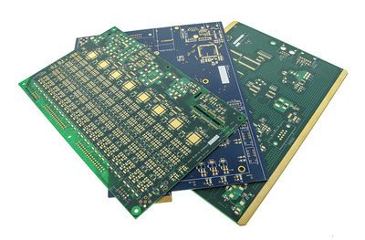
What are Multi-layer PCBs?
Multi-layer PCBs, or multi-layer printed circuit boards, are a type of PCB that consists of multiple layers of conductive material, typically copper, separated by insulating layers. These boards are designed to accommodate complex electronic circuits with high component density and intricate interconnections. By utilizing multiple layers, multi-layer PCBs offer several advantages over single or double-layer boards, including:
- Increased circuit density
- Improved signal integrity
- Reduced electromagnetic interference (EMI)
- Better heat dissipation
- Compact design
The Structure of Multi-layer PCBs
A typical multi-layer PCB consists of the following layers:
- Top layer: This is the outermost layer where components are mounted and traces are routed.
- Inner layers: These are the layers sandwiched between the top and bottom layers. They are used for signal routing, power distribution, and ground planes.
- Bottom layer: This is the opposite side of the top layer and is also used for component mounting and trace routing.
- Prepreg layers: These are the insulating layers that separate the conductive layers. They are made of a composite material, typically fiberglass, impregnated with a resin.
The number of layers in a multi-layer PCB can vary depending on the complexity of the circuit and the application requirements. Common multi-layer PCB configurations include 4-layer, 6-layer, 8-layer, and even up to 24-layer boards.
Advantages of Multi-layer PCBs
Increased Circuit Density
One of the primary advantages of multi-layer PCBs is their ability to accommodate high component density. By utilizing multiple layers for signal routing, more components can be placed on a single board, reducing the overall size of the electronic device. This is particularly important in applications where space is limited, such as smartphones, wearables, and IoT devices.
Improved Signal Integrity
Multi-layer PCBs offer improved signal integrity compared to single or double-layer boards. By using dedicated layers for power distribution and ground planes, the signal-to-noise ratio (SNR) can be significantly enhanced. This is because the power and ground layers act as shields, reducing the interference between signals on different layers. Additionally, multi-layer PCBs allow for controlled impedance routing, which helps maintain signal integrity over longer distances.
Reduced Electromagnetic Interference (EMI)
EMI is a common problem in electronic devices, caused by the unintentional radiation of electromagnetic energy from electronic components and traces. Multi-layer PCBs can help reduce EMI by using proper layer stackup and ground plane design. By placing signal layers between power and ground layers, the EMI can be effectively contained within the board. This is particularly important in applications that are sensitive to EMI, such as medical devices and aerospace systems.
Better Heat Dissipation
Multi-layer PCBs offer better heat dissipation compared to single or double-layer boards. This is because the multiple layers of copper and insulating material act as a heat sink, allowing the heat generated by electronic components to be efficiently dissipated. This is particularly important in high-power applications, such as power electronics and automotive systems.
Compact Design
By accommodating high component density and intricate interconnections, multi-layer PCBs enable compact electronic device designs. This is particularly important in applications where size and weight are critical factors, such as portable devices and aerospace systems.

Applications of Multi-layer PCBs
Multi-layer PCBs find applications in a wide range of industries and electronic devices. Some of the common applications include:
- Consumer electronics: Smartphones, tablets, laptops, and wearables
- Automotive electronics: Engine control units, infotainment systems, and advanced driver assistance systems (ADAS)
- Medical devices: Implantable devices, diagnostic equipment, and patient monitoring systems
- Aerospace and defense: Avionics, satellite communication systems, and radar systems
- Industrial automation: Programmable logic controllers (PLCs), human-machine interfaces (HMIs), and industrial sensors
- Telecommunications: Routers, switches, and base stations

Design Considerations for Multi-layer PCBs
Designing multi-layer PCBs involves several considerations to ensure optimal performance, reliability, and manufacturability. Some of the key design considerations include:
-
Layer stackup: The arrangement of conductive and insulating layers in a multi-layer PCB is crucial for signal integrity, EMI reduction, and manufacturability. Proper layer stackup design involves selecting the appropriate number of layers, the thickness of each layer, and the material properties of the insulating layers.
-
Signal routing: Signal routing in multi-layer PCBs involves selecting the appropriate trace width, spacing, and length to maintain signal integrity and minimize crosstalk. It also involves using controlled impedance routing techniques, such as microstrip and stripline, to match the impedance of the traces to the characteristic impedance of the system.
-
Power distribution: Power distribution in multi-layer PCBs involves using dedicated layers for power and ground planes. This helps reduce the voltage drop across the board and minimize the noise coupled to the signal layers. It also involves using proper decoupling and bypass capacitors to stabilize the power supply and reduce high-frequency noise.
-
Thermal management: Thermal management in multi-layer PCBs involves using appropriate thermal relief pads and vias to efficiently dissipate the heat generated by electronic components. It also involves selecting the appropriate copper thickness and dielectric material to minimize the thermal resistance of the board.
-
Manufacturing considerations: Designing multi-layer PCBs for manufacturability involves adhering to the design rules and guidelines specified by the PCB manufacturer. This includes selecting the appropriate minimum feature sizes, such as trace width and spacing, hole size, and annular ring, to ensure reliable and cost-effective manufacturing.

Multi-layer PCB Manufacturing Process
The manufacturing process for multi-layer PCBs involves several steps, including:
-
Inner layer processing: The inner layers of the PCB are etched with the required circuit patterns using photolithography and chemical etching processes.
-
Lamination: The inner layers are stacked together with the prepreg layers and copper foils, and the stack is laminated under high pressure and temperature to form a solid board.
-
Drilling: Through-holes and vias are drilled through the board to establish interconnections between layers.
-
Plating: The drilled holes are plated with copper to establish electrical connections between layers.
-
Outer layer processing: The outer layers of the PCB are etched with the required circuit patterns using photolithography and chemical etching processes.
-
Solder mask application: A solder mask layer is applied to the outer layers to protect the copper traces and prevent solder bridging.
-
Surface finish application: A surface finish, such as HASL, ENIG, or OSP, is applied to the exposed copper areas to protect them from oxidation and enhance solderability.
-
Electrical testing: The manufactured PCBs are electrically tested to ensure they meet the required specifications and functionality.
Comparison of Multi-layer PCBs with Single and Double-layer PCBs
| Parameter | Single-layer PCB | Double-layer PCB | Multi-layer PCB |
|---|---|---|---|
| Circuit density | Low | Medium | High |
| Signal integrity | Poor | Moderate | Excellent |
| EMI susceptibility | High | Moderate | Low |
| Heat dissipation | Poor | Moderate | Excellent |
| Design complexity | Simple | Moderate | High |
| Manufacturing cost | Low | Moderate | High |
As evident from the table, multi-layer PCBs offer several advantages over single and double-layer PCBs in terms of circuit density, signal integrity, EMI reduction, and heat dissipation. However, they also come with increased design complexity and manufacturing costs.
Future Trends in Multi-layer PCBs
The demand for multi-layer PCBs is expected to grow significantly in the coming years, driven by the increasing complexity of electronic devices and the need for miniaturization. Some of the future trends in multi-layer PCBs include:
-
High-density interconnect (HDI) PCBs: HDI PCBs are a type of multi-layer PCB that offers even higher circuit density and smaller feature sizes than traditional multi-layer PCBs. They are expected to find increasing applications in smartphones, wearables, and IoT devices.
-
Flexible and rigid-flex PCBs: Flexible and rigid-flex PCBs are a type of multi-layer PCB that combines flexible and rigid substrates to enable 3D packaging and improved reliability. They are expected to find increasing applications in wearables, medical devices, and aerospace systems.
-
Embedded components: Embedding passive components, such as resistors and capacitors, within the layers of a multi-layer PCB can significantly reduce the size and improve the performance of electronic devices. This trend is expected to gain momentum in the coming years, particularly in applications where size and weight are critical factors.
-
Advanced materials: The development of advanced materials, such as low-loss dielectrics and high-temperature laminates, is expected to enable the design of multi-layer PCBs with improved signal integrity, thermal stability, and reliability. These materials are particularly important in high-frequency and high-power applications, such as 5G telecommunications and electric vehicles.
Frequently Asked Questions (FAQ)
-
What is the difference between a multi-layer PCB and a single-layer PCB?
A multi-layer PCB consists of multiple layers of conductive material, typically copper, separated by insulating layers, while a single-layer PCB has only one conductive layer on a single insulating substrate. -
What are the advantages of using multi-layer PCBs?
Multi-layer PCBs offer several advantages, including increased circuit density, improved signal integrity, reduced EMI, better heat dissipation, and compact design. -
How many layers can a multi-layer PCB have?
The number of layers in a multi-layer PCB can vary depending on the complexity of the circuit and the application requirements. Common multi-layer PCB configurations include 4-layer, 6-layer, 8-layer, and even up to 24-layer boards. -
What are the design considerations for multi-layer PCBs?
Designing multi-layer PCBs involves several considerations, including layer stackup, signal routing, power distribution, thermal management, and manufacturing considerations. -
What are the future trends in multi-layer PCBs?
The future trends in multi-layer PCBs include HDI PCBs, flexible and rigid-flex PCBs, embedded components, and advanced materials.
Conclusion
Multi-layer PCBs are a critical technology in modern electronics, enabling the design of complex, high-density circuits with improved signal integrity, reduced EMI, and better thermal management. As electronic devices continue to become more sophisticated and miniaturized, the demand for multi-layer PCBs is expected to grow significantly. By understanding the advantages, design considerations, and manufacturing processes of multi-layer PCBs, engineers can design and develop electronic devices that are reliable, high-performing, and cost-effective. As future trends, such as HDI PCBs, flexible and rigid-flex PCBs, embedded components, and advanced materials, gain momentum, multi-layer PCBs are poised to play an even more crucial role in shaping the future of electronics.


Leave a Reply