What is a PCB?
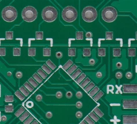
A Printed Circuit Board (PCB) is a thin board made of fiberglass or composite material that is used to mechanically support and electrically connect electronic components using conductive tracks, pads, and other features etched from copper sheets laminated onto a non-conductive substrate. PCBs are the foundation of modern electronic devices and are used in a wide range of applications, from simple single-layer boards to complex multilayer boards with thousands of components.
Types of PCBs
There are several types of PCBs, each with its own unique characteristics and applications:
-
Single-layer PCB: A single-layer PCB has only one layer of conductive material, typically copper, on one side of the substrate. These boards are simple, inexpensive, and suitable for low-complexity circuits.
-
Double-layer PCB: A double-layer PCB has two layers of conductive material, one on each side of the substrate. These boards offer more routing options and higher component density than single-layer boards.
-
Multi-layer PCB: A multi-layer PCB has three or more layers of conductive material, with insulating layers separating them. These boards are used for complex circuits that require high component density and intricate routing.
-
Flexible PCB: A flexible PCB is made using a flexible substrate, such as polyimide, allowing the board to bend and flex. These boards are used in applications where space is limited or where the board needs to conform to a particular shape.
-
Rigid-Flex PCB: A rigid-flex PCB combines the features of rigid and flexible PCBs, with rigid sections for mounting components and flexible sections for connecting them. These boards are used in applications that require both stability and flexibility.
Raw Materials Used in PCB Manufacturing
The raw materials used in PCB manufacturing play a crucial role in determining the quality, reliability, and performance of the final product. The following are the primary raw materials used in PCB manufacturing:
Substrate Materials
The substrate is the foundation of a PCB and provides the mechanical support and insulation for the conductive layers. The most common substrate materials are:
-
FR-4: FR-4 is a composite material made of woven fiberglass cloth with an epoxy resin binder. It is the most widely used substrate material due to its excellent mechanical, electrical, and thermal properties.
-
CEM-1: CEM-1 (Composite Epoxy Material) is a composite material made of a non-woven fiberglass mat with an epoxy resin binder. It is less expensive than FR-4 but has lower mechanical and thermal properties.
-
Polyimide: Polyimide is a high-performance polymer used in flexible PCBs. It has excellent mechanical, thermal, and electrical properties, making it suitable for applications that require high reliability and durability.
Conductive Materials
The conductive layers of a PCB are typically made of copper, which is an excellent conductor of electricity. The copper used in PCBs comes in two forms:
-
Copper Foil: Copper foil is a thin sheet of copper that is laminated onto the substrate. The thickness of the copper foil is typically measured in ounces per square foot (oz/ft²), with common thicknesses ranging from 0.5 oz/ft² to 2 oz/ft².
-
Copper Plating: Copper plating is the process of depositing a layer of copper onto the substrate using electroplating. This method is used to create the conductive tracks and pads on the PCB.
Solder Mask
The solder mask is a thin layer of polymer applied to the surface of the PCB to protect the copper traces from oxidation and to prevent solder bridges from forming during the soldering process. The solder mask also provides insulation between adjacent traces and improves the aesthetics of the board. The most common solder mask colors are green, red, and blue, but other colors are available for specific applications.
Silkscreen
The silkscreen is a layer of ink applied to the surface of the PCB to add text, logos, and other markings. The silkscreen is typically white, but other colors are available for specific applications. The silkscreen helps to identify components, provide assembly instructions, and improve the aesthetics of the board.

PCB Manufacturing Process
The PCB manufacturing process involves several steps, each of which is critical to ensuring the quality and reliability of the final product. The following are the primary steps in the PCB manufacturing process:
-
Design: The first step in the PCB manufacturing process is to design the board using specialized software. The design includes the layout of the components, the routing of the traces, and the placement of the vias and other features.
-
Fabrication: Once the design is complete, the fabrication process begins. The fabrication process involves several steps, including:
a. Copper Lamination: The substrate is laminated with a layer of copper foil on one or both sides.
b. Drilling: Holes are drilled in the board to accommodate through-hole components and vias.
c. Plating: The holes are plated with copper to create electrical connections between the layers.
d. Etching: The unwanted copper is removed using a chemical etching process, leaving only the desired traces and pads.
e. Solder Mask Application: The solder mask is applied to the board to protect the copper traces and to prevent solder bridges.
f. Silkscreen Printing: The silkscreen is printed onto the board to add text, logos, and other markings.
-
Assembly: Once the board is fabricated, the components are assembled onto the board using either through-hole or surface-mount technology. The components are soldered to the board using a soldering process, such as wave soldering or reflow soldering.
-
Testing: After the board is assembled, it is tested to ensure that it functions as intended. The testing process may include visual inspection, automated optical inspection (AOI), in-circuit testing (ICT), and functional testing.
-
Finishing: Finally, the board is finished by applying a protective coating, such as conformal coating or potting, to protect the components from environmental factors such as moisture, dust, and vibration.

Common PCB Defects and How to Prevent Them
Despite the advances in PCB manufacturing technology, defects can still occur during the manufacturing process. The following are some of the most common PCB defects and how to prevent them:
Solder Bridges
Solder bridges occur when excess solder creates an unintended connection between two or more pins or pads. To prevent solder bridges, ensure that the solder mask is properly aligned and that the solder paste is applied in the correct amount.
Cold Solder Joints
Cold solder joints occur when the solder does not melt completely, resulting in a weak or non-existent connection. To prevent cold solder joints, ensure that the soldering temperature is correct and that the components are properly aligned.
Tombstoning
Tombstoning occurs when a surface-mount component stands up on one end during the soldering process, creating an open circuit. To prevent tombstoning, ensure that the component pads are properly designed and that the solder paste is applied evenly.
Pad Lifting
Pad lifting occurs when the copper pad separates from the substrate during the soldering process. To prevent pad lifting, ensure that the copper is properly adhered to the substrate and that the soldering temperature is not too high.
Shorts and Opens
Shorts occur when two or more traces are unintentionally connected, while opens occur when a trace is broken or disconnected. To prevent shorts and opens, ensure that the etching process is properly controlled and that the traces are not damaged during handling.

FAQs
-
What is the difference between a single-layer and a multi-layer PCB?
A single-layer PCB has only one layer of conductive material, typically copper, on one side of the substrate. A multi-layer PCB has three or more layers of conductive material, with insulating layers separating them. Multi-layer PCBs are used for more complex circuits that require higher component density and more intricate routing. -
What is the purpose of the solder mask on a PCB?
The solder mask is a thin layer of polymer applied to the surface of the PCB to protect the copper traces from oxidation and to prevent solder bridges from forming during the soldering process. The solder mask also provides insulation between adjacent traces and improves the aesthetics of the board. -
What is the difference between through-hole and surface-mount technology?
Through-hole technology involves inserting the leads of components through holes drilled in the PCB and soldering them to pads on the opposite side. Surface-mount technology involves soldering components directly onto pads on the surface of the PCB. Surface-mount technology allows for higher component density and smaller board sizes. -
What is the purpose of testing a PCB after assembly?
Testing a PCB after assembly ensures that the board functions as intended and that there are no defects or issues that could affect its performance. Testing may include visual inspection, automated optical inspection (AOI), in-circuit testing (ICT), and functional testing. -
How can I prevent common PCB defects such as solder bridges and cold solder joints?
To prevent solder bridges, ensure that the solder mask is properly aligned and that the solder paste is applied in the correct amount. To prevent cold solder joints, ensure that the soldering temperature is correct and that the components are properly aligned. Proper design, handling, and process control can also help prevent other common PCB defects such as tombstoning, pad lifting, and shorts and opens.
Conclusion
PCBs are the backbone of modern electronics, and understanding the basic knowledge of PCB raw materials is essential for anyone involved in the design, manufacturing, or use of electronic devices. By selecting the appropriate substrate materials, conductive materials, solder mask, and silkscreen, and by following proper manufacturing processes and testing procedures, high-quality and reliable PCBs can be produced. Additionally, by being aware of common PCB defects and taking steps to prevent them, the overall quality and performance of PCBs can be further improved.


Leave a Reply