Introduction to PCB Design and Fabrication
Printed Circuit Boards (PCBs) are the backbone of modern electronics. They provide a platform for mounting and interconnecting electronic components, allowing for the creation of complex circuits in a compact and efficient manner. Whether you’re a hobbyist, a student, or a professional engineer, understanding how to design and fabricate custom PCBs is a valuable skill. In this comprehensive guide, we’ll walk you through the entire process of creating a custom PCB, from design to fabrication.
Understanding the Basics of PCB Design
Before diving into the PCB design process, it’s essential to understand the basic concepts and terminology associated with PCBs. Here are some key terms you should be familiar with:
- PCB Layer: PCBs can have multiple layers, each containing conductive traces and planes. The most common PCB types are single-layer, double-layer, and multi-layer boards.
- Trace: A trace is a conductive path that carries electrical signals between components on a PCB.
- Pad: A pad is a exposed area on a PCB where components are soldered.
- Via: A via is a conductive hole that connects traces on different layers of a PCB.
- Solder Mask: A solder mask is a protective layer applied to the PCB to prevent accidental short circuits during soldering.
- Silkscreen: Silkscreen is a layer of text and symbols printed on the PCB for identification and assembly purposes.
PCB Layers and Types
PCBs can be classified based on the number of layers they have:
| PCB Type | Number of Layers | Description |
|---|---|---|
| Single-layer | 1 | Has conductive traces on one side only |
| Double-layer | 2 | Has conductive traces on both sides |
| Multi-layer | 4, 6, 8, or more | Has multiple layers of conductive traces separated by insulation |
Multi-layer PCBs are used for complex designs that require a higher component density and better signal integrity.
Choosing the Right PCB Design Software
To create a custom PCB, you’ll need to use a PCB design software. There are many options available, ranging from free and open-source tools to professional-grade software. Here are some popular PCB design software choices:
- KiCad: A free and open-source PCB design suite that offers schematic capture, PCB layout, and 3D visualization.
- Eagle: A widely used PCB design software that offers a free version for non-commercial use and a paid version with advanced features.
- Altium Designer: A professional-grade PCB design software with a wide range of features and a steep learning curve.
- OrCAD: A powerful PCB design suite that includes schematic capture, PCB layout, and simulation tools.
When choosing a PCB design software, consider factors such as ease of use, learning resources, community support, and compatibility with your operating system.

Designing Your PCB Schematic
The first step in creating a custom PCB is to design the schematic. A schematic is a graphical representation of your circuit that shows how components are connected. Here’s how to design your PCB schematic:
- Create a new project: Start by creating a new project in your chosen PCB design software.
- Add components: Place the necessary components in the schematic editor. Most PCB design software have extensive libraries of common components.
- Connect components: Use wires to connect the components according to your circuit diagram. Ensure that the connections are correct and that there are no unintended short circuits.
- Add power and ground symbols: Place power and ground symbols in the schematic to indicate the power supply connections.
- Assign footprints: Assign footprints to each component in the schematic. A footprint is the physical representation of a component on the PCB.
- Perform error checking: Use the software’s error checking tools to identify and resolve any issues in the schematic, such as unconnected pins or missing components.
Laying Out Your PCB
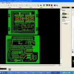
Once you have a complete schematic, you can move on to the PCB layout phase. This involves arranging the components on the PCB and routing the traces to connect them. Here’s how to lay out your PCB:
- Create a new PCB layout: Create a new PCB layout file in your PCB design software and import the schematic.
- Set the PCB dimensions: Define the size and shape of your PCB based on your project requirements.
- Place components: Arrange the components on the PCB, taking into account factors such as component size, orientation, and proximity to other components.
- Define the layer stack: Specify the number of layers in your PCB and assign them to different signal types (e.g., power, ground, signal).
- Route the traces: Use the software’s routing tools to create traces that connect the components. Consider factors such as trace width, spacing, and impedance matching.
- Add vias: Place vias to connect traces on different layers of the PCB.
- Add copper pours: Create copper pours (also known as fills) to provide a low-impedance path for power and ground connections.
- Perform design rule checks: Use the software’s design rule checking (DRC) tools to ensure that your PCB layout adheres to manufacturing constraints and best practices.
Preparing Your PCB for Fabrication
Before sending your PCB design to a fabrication house, you need to prepare the necessary files and documentation. Here’s what you need to do:
- Generate Gerber files: Export your PCB layout as a set of Gerber files. Gerber files are the industry standard format for PCB fabrication and contain information about the copper layers, solder mask, silkscreen, and drill holes.
- Create a drill file: Generate a drill file that specifies the location and size of all the holes in your PCB.
- Prepare a bill of materials (BOM): Create a list of all the components used in your PCB, including their part numbers, quantities, and suppliers.
- Write assembly instructions: If you plan to have your PCB assembled by a third party, provide clear assembly instructions, including component placement and orientation.
- Review and double-check: Carefully review all the files and documentation to ensure that they are accurate and complete.
Choosing a PCB Fabrication Service
With your PCB design files ready, it’s time to choose a PCB fabrication service. There are numerous PCB fabrication houses available, each with different capabilities, pricing, and turnaround times. Here are some factors to consider when selecting a PCB fabrication service:
- PCB specifications: Ensure that the fabrication house can meet your PCB specifications, such as the number of layers, minimum trace width, and hole size.
- Material options: Check if the fabricator offers the PCB materials you require, such as FR-4, high-frequency laminates, or flexible substrates.
- Turnaround time: Consider the fabrication house’s turnaround time and whether it meets your project deadlines.
- Pricing: Compare pricing among different fabricators, taking into account factors such as PCB complexity, quantity, and shipping costs.
- Customer support: Look for a fabricator with responsive customer support and clear communication channels.
Some popular PCB fabrication services include JLCPCB, PCBWay, OSH Park, and Seeed Studio.
Assembling Your PCB
Once you receive your fabricated PCBs, it’s time to assemble the components. PCB Assembly can be done by hand or using automated pick-and-place machines. If you’re assembling the PCB yourself, here are some tips:
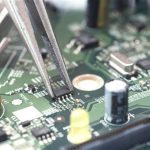
- Gather the necessary tools: You’ll need a soldering iron, solder, flux, tweezers, and a magnifying glass or microscope for inspection.
- Follow the assembly instructions: Refer to the assembly instructions you created earlier to ensure that components are placed correctly.
- Start with the smallest components: Begin by soldering the smallest components, such as resistors and capacitors, and work your way up to larger components.
- Use proper soldering techniques: Apply heat to both the pad and the component lead simultaneously, and feed solder into the joint. Avoid excessive heat or solder, which can lead to bridging or damage to the components.
- Inspect your work: Carefully inspect each solder joint for any defects, such as cold joints, bridging, or insufficient solder.
If you’re using an assembly service, provide them with the necessary files and instructions, and communicate any special requirements or considerations.
Testing and Debugging Your PCB
After assembling your PCB, it’s crucial to test and debug it to ensure that it functions as intended. Here are some steps to follow:
- Visual inspection: Perform a thorough visual inspection of the PCB, checking for any obvious defects, such as misaligned components, solder bridges, or damaged traces.
- Continuity testing: Use a multimeter to test for continuity between points that should be connected and ensure that there are no short circuits between points that should be isolated.
- Power-on testing: Apply power to the PCB and check for any signs of overheating, smoke, or unusual odors. Monitor the voltage levels at key points to ensure that they are within the expected range.
- Functional testing: Test the functionality of your PCB by applying inputs and measuring outputs. Compare the results with your design specifications and expectations.
- Debugging: If you encounter any issues during testing, use a systematic approach to isolate the problem. Check for loose connections, faulty components, or design errors. Use tools such as oscilloscopes, logic analyzers, or in-circuit debuggers to diagnose and resolve the issues.
Advanced PCB Design Techniques
As you gain experience in PCB design, you may want to explore advanced techniques to improve the performance, reliability, and manufacturability of your PCBs. Here are some advanced PCB design techniques to consider:
- High-speed design: When designing PCBs for high-speed applications, consider factors such as impedance matching, signal integrity, and crosstalk reduction. Use techniques such as differential signaling, microstrip or stripline routing, and ground planes to minimize signal distortion and noise.
- Electromagnetic compatibility (EMC): Ensure that your PCB design complies with EMC regulations to minimize electromagnetic interference (EMI) and susceptibility. Use techniques such as proper grounding, shielding, and filtering to reduce EMI and improve EMC performance.
- Thermal management: Consider the thermal characteristics of your PCB and components to prevent overheating and ensure reliable operation. Use techniques such as copper pours, thermal vias, and heat sinks to dissipate heat effectively.
- Design for manufacturing (DFM): Optimize your PCB design for manufacturability to reduce costs and improve yields. Follow DFM guidelines provided by your PCB fabrication house, such as minimum trace widths, clearances, and hole sizes. Use panelization techniques to maximize the number of PCBs per panel and minimize waste.
Frequently Asked Questions (FAQ)
- What is the difference between a schematic and a PCB layout?
-
A schematic is a graphical representation of a circuit that shows how components are connected, while a PCB layout is the physical arrangement of components and traces on a PCB.
-
Can I design a PCB without knowing how to code?
-
Yes, most PCB design software provides graphical user interfaces and libraries that allow you to design PCBs without writing code. However, some advanced features may require scripting or programming knowledge.
-
How much does it cost to fabricate a custom PCB?
-
The cost of PCB fabrication depends on factors such as the PCB size, number of layers, quantity, and turnaround time. Basic PCBs can cost as little as a few dollars per unit, while complex, high-volume PCBs can cost hundreds or thousands of dollars.
-
What is the typical turnaround time for PCB fabrication?
-
Turnaround times vary depending on the fabrication house and the complexity of the PCB. Standard turnaround times range from a few days to a couple of weeks. Some fabricators offer expedited services for faster turnaround times at an additional cost.
-
Do I need to have my PCB assembled professionally, or can I do it myself?
- You can assemble your PCB yourself if you have the necessary skills, tools, and equipment. However, for complex PCBs or high-volume production, it is often more cost-effective and reliable to use a professional PCB assembly service.
Conclusion
Designing and fabricating custom PCBs is a rewarding and essential skill for anyone involved in electronics. By following the steps outlined in this guide, you can create PCBs that meet your specific requirements and bring your electronic projects to life. Remember to start with a well-designed schematic, carefully lay out your PCB, and thoroughly test and debug your assembled board. As you gain experience, explore advanced techniques to improve the performance and manufacturability of your PCBs. With practice and perseverance, you’ll be able to create custom PCBs that are reliable, efficient, and tailored to your needs.
Leave a Reply