What are Blind Microvias and How Do They Enable Higher PCB Density?
A blind microvia is a tiny hole, typically 0.006-0.010 inches in diameter, that is laser-drilled from an outer layer of a printed circuit board (PCB) and connects to an inner layer without passing all the way through the board, as a through-hole via would. Because blind microvias only span 1-2 layers instead of the entire PCB thickness and have very small diameters, they enable much higher wiring density.
Consider the difference between a through-hole via and blind microvia:
| Property | Through-Hole Via | Blind Microvia |
|---|---|---|
| Diameter | 0.020-0.040 in | 0.006-0.010 in |
| Depth | Entire PCB thickness | 1-2 layers |
| Wiring density | Low | High |
| Cost | Low | Moderate |
The small size of blind microvias provides several advantages for high-density PCB designs:
- Reduced via hole size frees up routing space for more traces
- Blind vias can be placed directly under components instead of consuming space between them
- Multiple blind vias can be stacked to span more layers without increasing hole size
- High aspect ratio (depth to width) is achieved with laser drilling
These factors allow blind microvias to substantially increase the routing density and component density of complex PCBs. Smartphones, wearables, and other products that pack a lot of functionality into limited space rely heavily on blind microvias.
The Blind Microvia PCB Manufacturing Process
To build a PCB with blind microvias, a modified manufacturing process is used compared to standard Through-hole PCBs:
- The inner layers are fabricated with copper foil laminated to thin dielectric cores.
- The inner layer cores are laminated together with prepreg bonding sheets.
- Laser drilling machines are used to create the blind microvias in the outer layers down to the target inner layers. The laser vaporizes the dielectric material to form a hole.
- Electroless copper plating is applied to coat the microvia holes with a thin conductive seed layer.
- Electroplating builds up additional copper thickness in the holes and on the outer layer traces.
- Outer layers are etched to define circuit patterns.
- Solder mask and silkscreen are applied.
- Surface finish is plated (ENIG, HASL, IAg, etc.)
- The PCB is electrically tested.
The key enablers in this process are the use of laser drilling to create the microvias and the plating processes to make them conductive. Laser drilling allows the vias to be much smaller in diameter than what mechanical drills can achieve.

Laser Drilling Blind Microvias
Several types of lasers can be used to drill blind microvias in PCBs:
-
CO2 lasers: These gas lasers were commonly used in the early days of microvia adoption but have been largely replaced by better options. CO2 lasers have long pulse widths that can cause damage to the dielectric material around the via.
-
IR YAG lasers: Yttrium aluminum garnet lasers that emit infrared light are a popular choice for drilling microvias. They can achieve smaller hole sizes and higher aspect ratios than CO2.
-
UV YAG lasers: YAG lasers that output in the ultraviolet spectrum allow an even smaller focused spot size for the smallest microvias (below 0.005 in). The main drawback is slower drilling speed.
The choice of laser depends on the desired via size, acceptable drilling speed, heat effect on the dielectric, and cost. In general, UV YAG lasers provide the best quality but slowest throughput.
Proper laser drilling of blind microvias requires careful process control:
- Peak power, pulse width, and pulse repetition rate must be optimized
- The focal point of the beam must be consistent despite any warpage in the PCB
- Laser optics must be regularly cleaned and maintained
- Dielectric debris must be removed from the via after drilling
With the correct laser parameters and well-maintained equipment, microvias can be drilled with consistent size and shape. This is critical for achieving high yields in the subsequent plating processes.

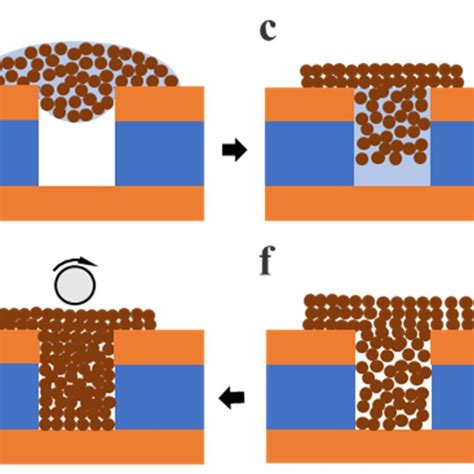
Plating Blind Microvias
Once the microvias have been laser-drilled, they need to be made conductive with copper plating. This happens in two stages:
-
Electroless copper: This is a chemical plating process that deposits a thin layer of copper (typically 0.0001-0.0003 in thick) on the surface of the via hole. The dielectric is first treated to make it receptive to the plating chemistry. Electroless copper provides the conductive “seed layer” required for the next plating step.
-
Electrolytic copper: Also known as “galvanic” or “electroplating”, this process uses an electric current to deposit thicker copper layers (0.0005-0.002 in) onto the electroless seed layer. The current is applied between the PCB and a copper anode submersed in an acidic copper sulfate bath. Copper ions are transferred from the anode to the cathode (the PCB) to build up the plating thickness.
The plating chemistry must be able to completely coat the inside of the microvia without any voids. Pulse plating, where the electric current is applied in on/off cycles, helps promote even plating distribution and prevents buildup at the shoulders of the via.
Smaller via sizes and higher aspect ratios make the plating process more challenging. A 0.006 in diameter microvia drilled through a 0.008 in thick dielectric layer has an aspect ratio of 1.33:1. Ratios up to 1:1 are routinely achievable but ultra-high density designs may push this to 1.5:1 or even 2:1. Plating these extreme vias requires very tight process controls.

Stacked Microvias for Higher Layer Counts
Blind microvias typically only span 1-2 PCB Layers, but some applications require connecting between multiple inner layers while still using the small via size. In this case, stacked microvias can be used.
Stacked microvias are two or more blind vias that are formed on top of each other to connect multiple layers. The laser drilling and plating processes are repeated to form each via in the stack. Some designs also utilize staggered microvias that are stacked but offset from each other.
The aspect ratio of stacked microvias can exceed 6:1, making them one of the most challenging HDI features to manufacture. Extremely tight laser drilling and plating process controls are required to produce consistent stacked microvias.
Microvia Reliability Concerns
While blind and buried microvias enable higher PCB densities, they also introduce new reliability concerns compared to through-hole vias. The main failure modes for microvias are:
- Separation between the bottom of the via and the target pad due to poor cleaning or low electroless copper coverage
- Barrel cracks due to mechanical or thermal stress
- Corners cracks where the barrel meets the surface copper
- Plating voids due to incomplete filling, especially in stacked microvias
IPC standards provide acceptance criteria for microvias and guidance on how to inspect them for defects. Cross-sectioning and microsectioning are commonly used to assess via quality on a sample basis. Electrical test methods such as 4-wire Kelvin and TDR can also detect some open and latent defects in microvias.
Following best practices during fabrication is key to achieving high microvia reliability:
- Drill microvias with the minimum diameter and aspect ratio required for the design
- Use an optimized laser drilling process that produces consistent hole shapes
- Thoroughly clean drilled vias to remove dielectric debris
- Electroless copper plate to a sufficient thickness for complete coverage
- Electrolytic copper plate to fill the entire via barrel without seams or voids
- Avoid stacked microvias if possible, or use filled stacked vias for the most demanding applications
Reliability testing should also be performed to qualify a microvia PCB design. Thermal cycling, environmental aging, and mechanical shock/vibration testing can reveal latent defects. However, a well-controlled fabrication process is the most important factor in microvia reliability.
Blind Microvia PCB Design Considerations
PCB designers should follow several guidelines to ensure manufacturability and reliability of designs with blind microvias:
- Consult with the PCB fabricator early in the design process to understand their capabilities and limitations
- Use the largest via size possible for the density requirements (preferably ≥0.006 in)
- Minimize the aspect ratio of the microvias (preferably ≤1:1)
- Avoid stacked microvias if possible, or limit the stack height
- Provide at least 4-5 mil of spacing between microvias and other features
- Specify a reference dielectric material to the fabricator to ensure laser drilling consistency
- Place microvias on a grid to allow optimal laser drilling throughput
- Limit the number of microvia layers in the stackup to control cost
Following these guidelines will help ensure high yields and high reliability in the final PCB Assembly.
FAQ
What is the difference between blind and buried microvias?
Blind microvias start at an outer layer and terminate at an inner layer. Buried microvias connect two inner layers without being visible on the surface. Blind vias are much more common than buried.
Are microvias more expensive than through-hole vias?
In general, yes. The special equipment and additional process steps required for microvias add cost compared to standard drilling and plating of through-holes. However, the higher wiring density enabled by microvias can provide an overall cost savings by reducing the number of layers in a PCB.
What type of design issues could eliminate the use of microvias?
Designs that have large or heavy components that induce high mechanical stress in the PCB may not be suitable for microvias. High power applications that generate a lot of heat could also be problematic for microvia reliability. In general, most applications can be designed to work with microvias as long as layout guidelines are followed.
What are the quality standards for microvias?
The two main standards that cover microvia PCBs are IPC-6016 and IPC-A-600. IPC-6016 defines three classes of end product, with increasing quality requirements from Class 1 to Class 3. IPC-A-600 provides visual acceptance criteria for microvias and other PCB structures based on cross-sectional analysis.
How can microvia reliability be tested?
Techniques such as microsectioning, scanning acoustic microscopy, and thermally-induced voltage alteration can be used to detect defects in microvias either before or after assembly. Functional testing of the final product, including accelerated thermal cycling and vibration testing, should also be performed to assess reliability under end-use conditions. Monitoring and control of the fabrication process is the best way to prevent microvia failures.
Conclusion
Blind microvias are an essential technology for enabling higher integration density in modern PCBs. By providing a means to interconnect layers without consuming surface area, microvias allow more space for routing traces and mounting components.
However, microvias also require more advanced manufacturing processes and introduce new reliability concerns. Laser drilling must produce precise holes with minimal dielectric damage, and electroplating must completely fill the high aspect ratio vias.
Following PCB design guidelines for microvias is critical to achieving high manufacturing yields and field reliability. By leveraging the density advantages of microvias while respecting their limitations, designers can pack more functionality into smaller form factors than ever before.


Leave a Reply