Introduction to PCB Layers
Printed Circuit Boards (PCBs) are essential components in modern electronic devices, providing a platform for electrical components to be mounted and interconnected. The number of layers in a PCB can vary depending on the complexity and requirements of the circuit design. In this article, we will explore the production process for different layers of PCB and understand the significance of each layer in the overall functioning of the board.
Types of PCB Layers
PCBs can be categorized based on the number of layers they contain. The most common types of PCBs are:
1. Single Layer PCB
Single layer PCBs, also known as single-sided PCBs, have conductive copper traces on only one side of the board. These PCBs are the simplest and most cost-effective option for basic electronic circuits.
2. Double Layer PCB
Double layer PCBs, or double-sided PCBs, have conductive copper traces on both sides of the board. The two layers are connected through conductive vias, allowing for more complex circuit designs and higher component density compared to single layer PCBs.
3. Multi-Layer PCB
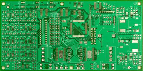
Multi-layer PCBs consist of three or more conductive layers, with insulating layers separating them. These PCBs are used for complex electronic devices that require high-density component placement and intricate circuit routing. The number of layers can range from four to twelve or more, depending on the application.
Production Process for PCB Layers
The production process for PCB layers involves several steps, each critical for ensuring the quality and functionality of the final product. The main steps in the PCB production process are:
1. PCB Design and Layout
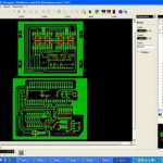
The first step in PCB production is designing the circuit schematic and creating the PCB layout using specialized software. The design includes determining the number of layers required, component placement, and routing of conductive traces.
2. Substrate Preparation
The substrate, typically made of fiberglass or other insulating materials, is cut to the desired size and shape. Holes are drilled for through-hole components and vias.
3. Copper Lamination
Copper foil is laminated onto the substrate using heat and pressure. The thickness of the copper foil varies depending on the current carrying requirements of the circuit.
4. Photoresist Application
A photosensitive resist is applied to the copper-laminated substrate. This resist will later be used to create the desired copper trace patterns.
5. Exposure and Development
The PCB layout is printed onto a transparent film, which is then placed on top of the photoresist-coated substrate. The board is exposed to UV light, hardening the exposed areas of the photoresist. The unexposed areas are then removed using a chemical developer, revealing the copper layer beneath.
6. Etching
The exposed copper is etched away using a chemical solution, leaving behind the desired copper trace patterns.
7. Resist Removal
The remaining photoresist is removed from the board, exposing the copper traces.
8. Layering and Lamination (for multi-layer PCBs)
For multi-layer PCBs, additional insulating layers and copper foil are laminated together, with conductive vias connecting the layers as required. This process is repeated until the desired number of layers is achieved.
9. Solder Mask Application
A solder mask is applied to the outer layers of the PCB, protecting the copper traces from oxidation and preventing solder bridges during component assembly.
10. Surface Finish
A surface finish, such as HASL (Hot Air Solder Leveling), ENIG (Electroless Nickel Immersion Gold), or OSP (Organic Solderability Preservative), is applied to the exposed copper areas to enhance solderability and protect the copper from oxidation.
11. Silkscreen Printing
The silkscreen layer is printed onto the PCB, providing text, logos, and component identifiers for easier assembly and troubleshooting.
12. Electrical Testing
The completed PCB undergoes electrical testing to ensure that all connections are properly made and that the board functions as intended.

Significance of Different PCB Layers
Each layer in a PCB serves a specific purpose in the overall functioning of the board. The significance of different PCB layers is as follows:
1. Conductive Layers
The conductive layers, typically made of copper, are responsible for carrying electrical signals between components. The thickness and width of the copper traces determine the current carrying capacity and signal integrity of the circuit.
2. Insulating Layers
The insulating layers, made of materials such as FR-4 or polyimide, provide electrical isolation between conductive layers. These layers prevent short circuits and ensure proper signal routing.
3. Power and Ground Planes
Dedicated power and ground planes in multi-layer PCBs provide a low-impedance path for power distribution and reduce electromagnetic interference (EMI). These planes also help maintain signal integrity by minimizing voltage drops and providing a stable reference for signal traces.
4. Signal Layers
Signal layers are responsible for routing the electrical signals between components. Proper signal layer design, including trace width, spacing, and impedance control, is crucial for maintaining signal integrity and minimizing crosstalk.
Advantages of Multi-Layer PCBs
Multi-layer PCBs offer several advantages over single and double layer PCBs:
-
Higher component density: Multi-layer PCBs allow for more components to be placed on a smaller board area, enabling the design of compact and complex electronic devices.
-
Improved signal integrity: Dedicated power and ground planes in multi-layer PCBs provide better signal integrity and reduce EMI.
-
Increased reliability: The additional layers in multi-layer PCBs offer more routing options and reduce the need for long, meandering traces, which can be prone to signal degradation and manufacturing defects.
-
Better thermal management: Multiple layers can help dissipate heat more effectively, improving the overall thermal performance of the device.
Challenges in Multi-Layer PCB Production
While multi-layer PCBs offer numerous benefits, their production also presents some challenges:
-
Higher production costs: The additional materials, processing steps, and equipment required for multi-layer PCB production result in higher costs compared to single or double layer PCBs.
-
Increased complexity: Designing and manufacturing multi-layer PCBs is more complex, requiring specialized knowledge and expertise in PCB layout, signal integrity, and manufacturing processes.
-
Longer lead times: The production of multi-layer PCBs typically takes longer due to the additional processing steps and the need for precise alignment of layers.
-
Potential for manufacturing defects: The increased complexity of multi-layer PCBs can lead to a higher risk of manufacturing defects, such as misaligned layers, inadequate lamination, or poor via connections.
Frequently Asked Questions (FAQ)
1. What is the difference between a single layer and a double layer PCB?
A single layer PCB has conductive copper traces on only one side of the board, while a double layer PCB has conductive traces on both sides. Double layer PCBs offer more routing options and higher component density compared to single layer PCBs.
2. How many layers can a multi-layer PCB have?
A multi-layer PCB can have anywhere from four to twelve or more layers, depending on the complexity and requirements of the electronic device.
3. What materials are used for the insulating layers in a PCB?
Common materials used for insulating layers in PCBs include FR-4 (a composite material made of fiberglass and epoxy resin) and polyimide.
4. Why are dedicated power and ground planes important in multi-layer PCBs?
Dedicated power and ground planes in multi-layer PCBs provide a low-impedance path for power distribution, reduce electromagnetic interference (EMI), and help maintain signal integrity by minimizing voltage drops and providing a stable reference for signal traces.
5. Are multi-layer PCBs more expensive than single or double layer PCBs?
Yes, multi-layer PCBs are generally more expensive to produce than single or double layer PCBs due to the additional materials, processing steps, and equipment required. However, the benefits of multi-layer PCBs, such as higher component density, improved signal integrity, and better thermal management, often justify the increased cost for complex electronic devices.
Conclusion
Understanding the production process for different layers of PCB is crucial for designing and manufacturing reliable and high-performance electronic devices. The number of layers in a PCB directly influences its functionality, complexity, and cost. Single and double layer PCBs are suitable for simple electronic circuits, while multi-layer PCBs are essential for more complex devices that require high component density and superior signal integrity.
By comprehending the significance of each layer and the challenges involved in multi-layer PCB production, engineers and designers can make informed decisions when creating PCB layouts and selecting the appropriate number of layers for their projects. As electronic devices continue to advance and become more sophisticated, the demand for multi-layer PCBs is expected to grow, driving innovations in PCB design and manufacturing technologies.
Leave a Reply