Introduction to Diptrace
Diptrace is a powerful and user-friendly electronic design automation (EDA) software package that allows users to create professional-quality printed circuit board (PCB) designs. Whether you’re a beginner or an experienced PCB designer, Diptrace offers a comprehensive set of tools and features to help you bring your electronic projects to life.
In this Diptrace Guide, we’ll walk you through the process of learning and mastering Diptrace, from the basics to advanced techniques. By the end of this article, you’ll have a solid understanding of how to use Diptrace to create high-quality PCB designs efficiently and effectively.
Getting Started with Diptrace
Downloading and Installing Diptrace
To get started with Diptrace, you’ll need to download and install the software on your computer. Visit the official Diptrace website (https://diptrace.com/) and navigate to the Downloads section. Choose the appropriate version for your operating system (Windows, macOS, or Linux) and follow the installation instructions provided.
Understanding the Diptrace User Interface
Once you’ve installed Diptrace, it’s time to familiarize yourself with the user interface. The main window of Diptrace consists of several key areas:
- Menu Bar: Located at the top of the window, the menu bar provides access to various commands and settings.
- Toolbars: Below the menu bar, you’ll find toolbars containing frequently used tools and functions.
- Workspace: The central area of the window where you’ll design your PCBs and schematics.
- Panels: On the left and right sides of the workspace, you’ll find panels that display libraries, properties, and other information.
Configuring Diptrace Preferences
Before diving into your first project, it’s a good idea to configure Diptrace’s preferences to suit your needs. To access the preferences, go to the “Tools” menu and select “Preferences.” Here, you can customize settings such as units, grid size, default trace width, and more.
Creating a New Project in Diptrace
Starting a New Project
To start a new project in Diptrace, follow these steps:
- Go to the “File” menu and select “New Project.”
- Choose a project template or select “Empty Project” to start from scratch.
- Enter a name for your project and select a location to save it.
- Click “OK” to create the new project.
Setting Up the Project Properties
Once you’ve created a new project, you can set up its properties to define the basic parameters of your PCB design. To access the project properties, go to the “File” menu and select “Project Properties.” Here, you can specify the following:
- Board size and shape
- Number of layers
- Copper thickness
- Dielectric constant
- Trace width and clearance
- Via size and drill diameter

Designing the Schematic
Creating a New Schematic
In Diptrace, the first step in creating a PCB is to design the schematic. To create a new schematic, follow these steps:
- In the project tree, right-click on the “Schematics” folder and select “Add Schematic.”
- Enter a name for your schematic and click “OK.”
- The new schematic will open in the workspace.
Adding Components to the Schematic
To add components to your schematic, you’ll need to use the component libraries provided by Diptrace or create your own custom components. To add a component:
- Open the “Components” panel on the left side of the window.
- Browse the libraries to find the desired component or use the search function to locate it quickly.
- Drag and drop the component from the library onto the schematic workspace.
- Repeat this process for all the components in your design.
Connecting Components with Wires
Once you’ve placed your components on the schematic, you’ll need to connect them using wires. To create a wire:
- Select the “Wire” tool from the toolbar or press the “W” key on your keyboard.
- Click on the starting point of the wire (usually a component pin) and drag the mouse to the ending point.
- Release the mouse button to complete the wire.
- Repeat this process to connect all the necessary components.
Assigning Net Names and Labels
To help identify and organize the connections in your schematic, you can assign net names and labels to the wires. To assign a net name:
- Double-click on a wire to open the “Wire Properties” dialog.
- Enter a name for the net in the “Name” field.
- Click “OK” to apply the changes.
To add a label to a wire:
- Select the “Label” tool from the toolbar.
- Click on the wire where you want to place the label.
- Enter the label text and press Enter.
Checking the Schematic for Errors
Before proceeding to the PCB layout, it’s essential to check your schematic for errors. Diptrace provides a built-in electrical rule check (ERC) tool to help you identify and resolve issues. To run an ERC:
- Go to the “Tools” menu and select “ERC.”
- In the ERC dialog, select the desired rule set and click “Run.”
- Diptrace will display any errors or warnings found in the schematic.
- Double-click on an error in the list to locate it on the schematic.
- Make the necessary corrections and rerun the ERC until no errors are found.
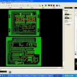
Designing the PCB Layout
Creating a New PCB
Once your schematic is complete and error-free, you can create a new PCB layout. To create a new PCB:
- In the project tree, right-click on the “PCBs” folder and select “Add PCB.”
- Enter a name for your PCB and click “OK.”
- The new PCB will open in the workspace.
Importing the Netlist
To transfer the connectivity information from your schematic to the PCB layout, you’ll need to import the netlist. To import the netlist:
- In the PCB workspace, go to the “Tools” menu and select “Import Netlist.”
- Select the schematic you want to import and click “OK.”
- Diptrace will place the components and nets on the PCB according to the schematic.
Placing Components
After importing the netlist, you’ll need to arrange the components on the PCB. To place a component:
- Select the “Move” tool from the toolbar or press the “M” key on your keyboard.
- Click and drag a component to its desired location on the PCB.
- Use the “Rotate” tool or press the “R” key to orient the component as needed.
- Repeat this process for all the components on the PCB.
Routing Traces
With the components placed, you can begin routing the traces to connect them according to the schematic. To route a trace:
- Select the “Route” tool from the toolbar or press the “X” key on your keyboard.
- Click on the starting pad and drag the mouse to the ending pad.
- Diptrace will automatically route the trace, following the design rules you’ve set up.
- Repeat this process to route all the necessary connections.
Adding Vias and Copper Pours
To connect traces on different layers of the PCB, you’ll need to use vias. To add a via:
- Select the “Via” tool from the toolbar.
- Click on the location where you want to place the via.
- Adjust the via properties (size, drill, layers) as needed.
To create copper pours for power or ground planes:
- Select the “Copper Pour” tool from the toolbar.
- Click on the area where you want to create the pour.
- In the “Copper Pour Properties” dialog, select the desired layer, net name, and other settings.
- Click “OK” to create the copper pour.
Running Design Rule Checks (DRC)
To ensure that your PCB layout meets the manufacturing requirements and design rules, you should run a design rule check (DRC). To run a DRC:
- Go to the “Tools” menu and select “DRC.”
- In the DRC dialog, select the desired rule set and click “Run.”
- Diptrace will display any errors or warnings found in the PCB layout.
- Double-click on an error in the list to locate it on the PCB.
- Make the necessary corrections and rerun the DRC until no errors are found.
Generating Manufacturing Files
Creating Gerber Files
Once your PCB layout is complete and has passed the DRC, you’ll need to generate Gerber files for manufacturing. Gerber files are the industry standard format for PCB Fabrication. To create Gerber files:
- Go to the “File” menu and select “Export.”
- In the “Export” dialog, select “Gerber” as the format.
- Configure the Gerber settings (layers, apertures, etc.) according to your manufacturer’s requirements.
- Click “Export” to generate the Gerber files.
Generating Drill Files
In addition to Gerber files, you’ll also need to generate drill files that specify the locations and sizes of holes on the PCB. To generate drill files:
- Go to the “File” menu and select “Export.”
- In the “Export” dialog, select “NC Drill” as the format.
- Configure the drill settings (units, format, etc.) according to your manufacturer’s requirements.
- Click “Export” to generate the drill files.
Creating a Bill of Materials (BOM)
A bill of materials (BOM) is a list of all the components used in your PCB design. To create a BOM:
- Go to the “Reports” menu and select “BOM.”
- In the BOM dialog, select the desired output format (CSV, Excel, etc.).
- Configure the BOM settings (columns, sorting, etc.) as needed.
- Click “Generate” to create the BOM file.
Advanced Diptrace Techniques
Using Hierarchical Schematics
For complex designs, you can use hierarchical schematics to organize your project into smaller, more manageable sub-circuits. To create a hierarchical schematic:
- Create a new schematic for the sub-circuit.
- Design the sub-circuit as a standalone schematic.
- In the main schematic, add a hierarchical block that represents the sub-circuit.
- Connect the hierarchical block to the rest of the schematic using ports.
Creating Custom Components
If you can’t find a specific component in the Diptrace libraries, you can create your own custom component. To create a custom component:
- Go to the “Tools” menu and select “Component Editor.”
- In the Component Editor, design the schematic symbol and PCB footprint for your component.
- Save the component to a library for future use.
Using Scripting and Automation
Diptrace supports scripting and automation through its built-in Diptrace Scripting Language (DSL). With DSL, you can automate repetitive tasks, create custom commands, and extend Diptrace’s functionality. To learn more about DSL, refer to the Diptrace Scripting Language manual.
Frequently Asked Questions (FAQ)
-
Q: Can I import designs from other EDA software into Diptrace?
A: Yes, Diptrace supports importing designs from various formats, including Eagle, Altium, KiCad, and OrCAD. To import a design, go to the “File” menu and select “Import.” -
Q: How do I update components in my schematic and PCB layout simultaneously?
A: Diptrace supports forward and backward annotation, which allows you to update components in both the schematic and PCB layout. To update components, go to the “Tools” menu and select “Forward Annotation” or “Backward Annotation.” -
Q: Can I create multi-page schematics in Diptrace?
A: Yes, Diptrace allows you to create multi-page schematics. To add a new page, go to the “Page” menu and select “Add Page.” You can navigate between pages using the tabs at the bottom of the schematic workspace. -
Q: How do I create a custom PCB shape in Diptrace?
A: To create a custom PCB shape, go to the “Objects” menu and select “Board Outline.” Use the drawing tools to create the desired shape, or import a DXF file containing the outline. -
Q: Can I collaborate with other designers on a Diptrace project?
A: Yes, Diptrace supports collaboration through its “Diptrace Team” feature. With Diptrace Team, multiple designers can work on the same project simultaneously, with real-time synchronization and version control.
Conclusion
Diptrace is a powerful and versatile EDA software that offers a wide range of features for designing professional-quality PCBs. By following this step-by-step guide, you’ll be well on your way to mastering Diptrace and creating impressive electronic projects.
Remember to start with a solid foundation in the basics, such as creating schematics, placing components, and routing traces. As you gain more experience, explore advanced techniques like hierarchical schematics, custom components, and scripting to streamline your workflow and tackle more complex designs.
With practice and perseverance, you’ll soon be designing PCBs like a pro using Diptrace. Happy designing!


Leave a Reply