What is a PCB Etcher?
A PCB (Printed Circuit Board) etcher is a machine used to create custom PCBs by selectively removing copper from a copper-clad board. This process is called etching and is an essential step in the PCB Fabrication process. PCB etchers come in various sizes and types, ranging from simple DIY setups to advanced industrial machines.
Types of PCB Etchers
There are two main types of PCB etchers:
- Chemical Etchers
- Mechanical Etchers
Chemical Etchers
Chemical etchers use a chemical solution, typically ferric chloride or ammonium persulfate, to dissolve the unwanted copper from the PCB. The PCB is immersed in the etching solution, and the exposed copper is gradually removed, leaving behind the desired circuit pattern.
| Advantages | Disadvantages |
|---|---|
| Inexpensive | Messy and potentially hazardous |
| Simple setup | Slower than mechanical etching |
| Suitable for small-scale production | Requires proper disposal of chemicals |
Mechanical Etchers
Mechanical etchers use physical means, such as CNC milling or laser etching, to remove the unwanted copper from the PCB. These machines are more precise and faster than chemical etchers but are also more expensive and complex to set up.
| Advantages | Disadvantages |
|---|---|
| High precision | Expensive |
| Fast etching process | Complex setup |
| Suitable for large-scale production | Requires specialized equipment |
How to Make a DIY PCB Etcher
Making a DIY PCB etcher is a cost-effective way to create custom PCBs at home. Here’s a step-by-step guide on how to make a simple chemical PCB etcher:
Materials Needed
- Plastic container
- Aquarium air pump
- Air stone
- Tubing
- Ferric chloride or ammonium persulfate
- Protective gloves and goggles
- Copper-clad PCB
- Printed circuit design
- Transparency film
- UV exposure unit (optional)
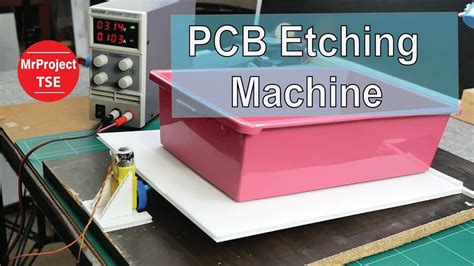
Step 1: Prepare the Etching Container
- Choose a plastic container large enough to accommodate your PCB.
- Drill two holes in the container’s lid: one for the air tubing and another for ventilation.
- Insert the air stone into the container and connect it to the air pump using the tubing.
Step 2: Create the Circuit Design
- Design your circuit using PCB design software or draw it manually.
- Print the circuit design onto a transparency film using a laser printer.
- If using a UV exposure unit, place the transparency film on the copper-clad PCB and expose it to UV light for the recommended time.
- Develop the PCB in a sodium hydroxide solution to remove the unexposed photoresist.
Step 3: Etch the PCB
- Put on protective gloves and goggles.
- Pour the etching solution into the prepared container, following the manufacturer’s instructions.
- Place the developed PCB into the etching solution, ensuring it is fully submerged.
- Turn on the air pump to agitate the solution and speed up the etching process.
- Monitor the etching progress closely. Remove the PCB once all the unwanted copper has been dissolved.
Step 4: Clean and Finish the PCB
- Rinse the etched PCB thoroughly with water.
- Remove the remaining photoresist using acetone or a specialized photoresist remover.
- Drill any necessary holes for components.
- Apply a solder mask and silkscreen (optional) for a professional finish.

Tips for Successful PCB Etching
- Always wear protective gear when handling etching chemicals.
- Ensure proper ventilation in your work area.
- Dispose of used etching solutions according to local regulations.
- Regularly maintain and clean your etching equipment.
- Experiment with different etching times and solution concentrations to achieve optimal results.

Frequently Asked Questions (FAQ)
1. What is the best chemical for PCB etching?
The two most common chemicals used for PCB etching are ferric chloride and ammonium persulfate. Ferric chloride is more widely available and easier to use, while ammonium persulfate is less messy and produces less waste.
2. Can I reuse the etching solution?
Yes, etching solutions can be reused multiple times. However, the etching process will become slower as the solution becomes saturated with copper. It’s essential to monitor the solution’s effectiveness and replace it when necessary.
3. How long does the etching process take?
The etching time depends on various factors, such as the strength of the etching solution, the thickness of the copper layer, and the complexity of the circuit design. On average, the process can take anywhere from 10 to 45 minutes.
4. Is it necessary to use a UV exposure unit?
No, a UV exposure unit is not strictly necessary. You can use the toner transfer method, which involves printing the circuit design onto glossy paper and transferring it to the PCB using heat and pressure. However, using a UV exposure unit results in higher-quality PCBs with finer details.
5. Can I make double-sided PCBs with a DIY etcher?
Yes, it is possible to make double-sided PCBs with a DIY etcher. However, it requires more precise alignment and registration of the circuit designs on both sides of the PCB. It’s recommended to use alignment pins or specialized double-sided PCB Holders to ensure proper registration.

Conclusion
Creating a DIY PCB etcher is an excellent way to prototype and manufacture custom PCBs at home. By following the steps outlined in this article and taking the necessary safety precautions, you can build a simple and effective chemical etcher that will serve your PCB fabrication needs. As you gain experience and confidence, you can explore more advanced etching techniques and even consider investing in a mechanical etcher for higher-precision projects.


Leave a Reply