Introduction to PCBA Quality Criteria
Printed Circuit Board Assembly (PCBA) is a crucial process in the manufacturing of electronic devices. The quality of the PCBA directly affects the performance, reliability, and longevity of the final product. To ensure high-quality PCBAs, it is essential to establish a set of quality criteria and defect classifications. This article will provide a comprehensive overview of the criteria for quality defects of PCBA, helping manufacturers and quality control professionals identify and address issues effectively.
Types of PCBA Defects
PCBA defects can be categorized into several types based on their nature and impact on the functionality of the assembled board. The main categories of PCBA defects include:
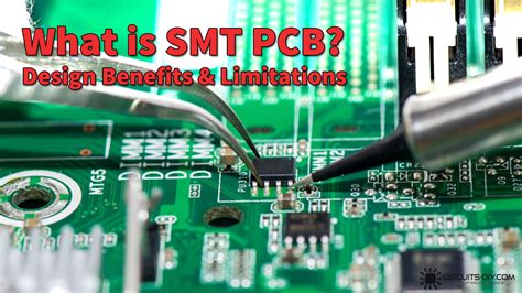
1. Soldering Defects
Soldering defects are among the most common issues encountered in PCBA. These defects can lead to poor electrical connections, shorts, or open circuits. Some examples of soldering defects are:
- Bridging: Unwanted connection between two or more solder joints
- Insufficient solder: Inadequate amount of solder, resulting in a weak or open connection
- Excess solder: Excessive amount of solder, potentially causing shorts or impeding proper component placement
- Cold solder joint: A dull, porous, or cracked solder joint due to improper soldering techniques or temperatures
- Tombstoning: A component lifting off the board due to uneven heating or solder surface tension
2. Component Placement Defects
Component placement defects occur when components are not correctly positioned or oriented on the PCB. These defects can cause functional issues or hinder the assembly process. Examples of component placement defects include:
- Misalignment: Components not placed accurately in their designated locations
- Incorrect orientation: Components rotated or flipped, leading to improper connections
- Missing components: Components left out during the assembly process
- Damaged components: Components damaged during placement or handling
3. PCB Defects
PCB defects are issues related to the printed circuit board itself, which can affect the overall quality and reliability of the PCBA. Some common PCB defects are:
- Short circuits: Unwanted electrical connections between conductive paths
- Open circuits: Broken or disconnected conductive paths
- Contamination: Foreign particles or residues on the PCB surface
- Delamination: Separation of PCB layers due to poor bonding or stress
- Warpage: Distortion of the PCB due to thermal or mechanical stress
4. Visual Defects
Visual defects are cosmetic issues that may not directly impact the functionality of the PCBA but can indicate underlying problems or affect the overall appearance of the product. Examples of visual defects include:
- Scratches or dents on the PCB surface
- Discoloration or stains on components or the PCB
- Incorrect or missing markings or labels
- Poor conformal coating application

PCBA Quality Inspection Methods
To identify and address PCBA defects, various inspection methods can be employed at different stages of the assembly process. These methods help ensure that defects are caught early and corrected before the PCBA moves to the next stage or is integrated into the final product.
1. Visual Inspection
Visual inspection is the most basic and widely used method for detecting PCBA defects. Trained inspectors examine the assembled boards under magnification to identify visible defects such as soldering issues, component placement errors, or surface defects. Visual inspection can be performed manually or using automated optical inspection (AOI) systems.
2. Automated Optical Inspection (AOI)
AOI systems use high-resolution cameras and advanced image processing algorithms to detect defects on the PCBA. These systems can quickly scan the entire board and compare it to a reference image, identifying any discrepancies or anomalies. AOI is particularly effective in detecting component placement defects, solder bridge


Leave a Reply