What is a PCB Layer Stack-Up?
The PCB layer stack-up refers to the arrangement of copper and insulating layers that make up a printed circuit board. It defines the number of layers, their order, the materials used for each layer, and the thickness of the copper and dielectric.
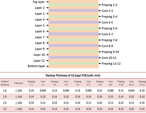
A typical PCB consists of the following layers:
- Solder mask (top and bottom)
- Copper layers (signal, power, and ground)
- Core dielectric material (FR-4, Rogers, etc.)
- Prepreg (pre-impregnated) dielectric material
The choice of layer stack-up depends on various factors such as the complexity of the circuit, signal integrity requirements, power requirements, cost, and manufacturing capabilities.
Importance of Proper Layer Stack-Up Design
A well-designed PCB layer stack-up is crucial for several reasons:
-
Signal integrity: The layer stack-up affects the characteristic impedance, crosstalk, and electromagnetic interference (EMI) of the PCB. Proper design ensures that signals maintain their integrity and minimize interference.
-
Power integrity: The placement of power and ground planes in the stack-up affects the power distribution network’s impedance and the board’s ability to handle current.
-
Manufacturability: The choice of materials, layer thicknesses, and the number of layers affect the ease and cost of manufacturing the PCB.
-
Reliability: A proper layer stack-up ensures that the PCB can withstand the stresses of assembly, handling, and operation, minimizing the risk of failures.

Factors to Consider When Designing a Layer Stack-Up
Number of Layers
The number of layers in a PCB is determined by the complexity of the circuit and the routing requirements. A simple circuit may only require two layers (top and bottom), while a complex design may need eight or more layers.
The most common layer counts are:
- 2 layers
- 4 layers
- 6 layers
- 8 layers
- 10 layers
- 12 layers
As the number of layers increases, so does the cost and complexity of manufacturing.
Layer Arrangement
The arrangement of layers in the stack-up depends on the signal integrity and power requirements of the design. A typical 4-layer PCB stack-up may look like this:
| Layer | Material | Thickness (mil) |
|---|---|---|
| Top Solder Mask | Solder Mask | 0.5 |
| Top Copper | Copper | 1.4 |
| Core | FR-4 | 47 |
| Inner Layer 1 (Ground) | Copper | 1.0 |
| Core | FR-4 | 47 |
| Inner Layer 2 (Power) | Copper | 1.0 |
| Core | FR-4 | 47 |
| Bottom Copper | Copper | 1.4 |
| Bottom Solder Mask | Solder Mask | 0.5 |
In this example, the signal layers are on the top and bottom, while the ground and power planes are on the inner layers. This arrangement provides good signal integrity and power distribution.
Copper Thickness
The thickness of the copper layers affects the current carrying capacity and the impedance of the traces. Thicker copper allows for higher current but also increases the cost and weight of the PCB.
Common copper thicknesses are:
- 0.5 oz (0.7 mil or 18 μm)
- 1 oz (1.4 mil or 35 μm)
- 2 oz (2.8 mil or 70 μm)
- 3 oz (4.2 mil or 105 μm)
The choice of copper thickness depends on the current requirements and the desired impedance of the traces.
Dielectric Material and Thickness
The dielectric material is the insulating layer between the copper layers. The most common dielectric material is FR-4, a glass-reinforced epoxy laminate. Other materials, such as Rogers or Isola, may be used for high-frequency or high-speed applications.
The thickness of the dielectric affects the impedance of the traces and the overall thickness of the PCB. Thinner dielectrics allow for closer spacing of traces and higher layer counts, but they also increase the risk of manufacturing defects and signal integrity issues.
Common dielectric thicknesses are:
- 4 mil (0.1 mm)
- 6 mil (0.15 mm)
- 8 mil (0.2 mm)
- 10 mil (0.25 mm)
- 12 mil (0.3 mm)
The choice of dielectric thickness depends on the desired impedance, layer count, and manufacturing capabilities.

Designing for Signal Integrity
Signal integrity is a critical consideration in PCB design, especially for high-speed digital circuits. The layer stack-up plays a significant role in maintaining signal integrity.
Controlled Impedance
Controlled impedance is the practice of designing traces to have a specific characteristic impedance, typically 50 ohms for single-ended signals and 100 ohms for differential pairs. This is achieved by carefully selecting the trace width, dielectric thickness, and copper thickness.
The characteristic impedance of a trace is given by:
Z₀ = 87 / √(ε_r + 1.41) × ln(5.98 × h / (0.8 × w + t))
Where:
– Z₀ is the characteristic impedance in ohms
– ε_r is the relative permittivity of the dielectric
– h is the dielectric thickness in mils
– w is the trace width in mils
– t is the copper thickness in mils
By using a PCB stack-up calculator or impedance calculator, designers can determine the appropriate trace dimensions for a given impedance and dielectric material.
Crosstalk
Crosstalk is the unwanted coupling of signals between adjacent traces. It can cause signal integrity issues and lead to malfunctions in the circuit.
To minimize crosstalk, designers can:
- Increase the spacing between traces
- Use differential signaling instead of single-ended signaling
- Place ground planes adjacent to signal layers
- Use guard traces or ground fills between sensitive traces
By carefully designing the layer stack-up and trace geometry, designers can reduce crosstalk and improve signal integrity.
EMI and EMC
Electromagnetic interference (EMI) and electromagnetic compatibility (EMC) are concerns in PCB design, particularly for products that must meet regulatory requirements.
To minimize EMI and improve EMC, designers can:
- Use ground planes to provide shielding and a low-impedance return path for signals
- Minimize the loop area of current paths by placing return paths close to signal traces
- Use stripline or microstrip trace geometries to provide additional shielding
- Avoid splitting ground planes, which can create slot antennas
By considering EMI and EMC in the layer stack-up design, designers can create PCBs that are less likely to cause or be affected by electromagnetic interference.

Designing for Power Integrity
Power integrity is another critical consideration in PCB design. The layer stack-up plays a significant role in ensuring that power is distributed efficiently and with minimal noise.
Power and Ground Planes
Power and ground planes are solid copper layers that provide a low-impedance distribution network for power and ground. They also provide shielding and a reference plane for signals.
In a typical layer stack-up, power and ground planes are placed adjacent to each other, with a thin dielectric layer in between. This creates a distributed capacitance that helps to reduce power supply noise and provide a stable reference voltage for signals.
Decoupling Capacitors
Decoupling capacitors are used to provide a local source of charge for ICs and to reduce power supply noise. They are typically placed close to the power pins of ICs and connected to the power and ground planes with short, low-impedance traces.
The placement and selection of decoupling capacitors depend on the frequency and current requirements of the ICs. In general, higher frequencies require smaller capacitors placed closer to the ICs, while lower frequencies can use larger capacitors placed farther away.
Splitting Power and Ground Planes
In some cases, it may be necessary to split power and ground planes to accommodate different voltage levels or to isolate sensitive circuits. However, splitting planes can create discontinuities that can cause signal integrity and EMI issues.
To minimize these issues, designers should:
- Keep splits as short and straight as possible
- Avoid splitting planes under sensitive traces or components
- Use stitching capacitors to provide a low-impedance connection between split planes
- Use ground bridges or stitching vias to maintain continuity between split ground planes
By carefully designing the power and ground planes in the layer stack-up, designers can ensure good power integrity and minimize issues related to power supply noise and voltage drops.
Manufacturing Considerations
The layer stack-up design also affects the manufacturability and cost of the PCB. Designers should consider the following factors when designing the stack-up:
- Number of layers: More layers increase the complexity and cost of manufacturing.
- Material availability: Some specialized dielectric materials may be more expensive or have longer lead times than standard FR-4.
- Minimum feature size: Smaller traces and spaces require more precise manufacturing equipment and may increase the cost.
- Aspect ratio: The ratio of the hole diameter to the board thickness affects the reliability of plated through-holes. A ratio of 1:8 or greater is recommended.
- Copper thickness: Thicker copper layers may require longer etching times and may be more difficult to manufacture.
By considering these factors and working closely with the PCB manufacturer, designers can create layer stack-ups that are cost-effective and easy to manufacture.
Frequently Asked Questions
1. What is the most common layer count for PCBs?
The most common layer count for PCBs is four layers. This provides a good balance between signal integrity, power distribution, and cost. Two-layer boards are used for simple designs, while six or more layers are used for more complex designs with higher speed or power requirements.
2. What is the difference between a core and prepreg dielectric?
A core dielectric is a solid, pre-cured material that is used to provide structural support for the PCB. Prepreg (pre-impregnated) dielectric is a partially cured material that is used to bond the layers together during the lamination process. Prepreg is more flexible and conformable than core material, allowing it to fill in gaps and create a strong bond between layers.
3. How does the dielectric constant affect the PCB design?
The dielectric constant (Dk) is a measure of a material’s ability to store electric energy. In PCBs, the dielectric constant affects the speed of signals and the characteristic impedance of traces. A higher Dk results in slower signal propagation and lower impedance, while a lower Dk results in faster signal propagation and higher impedance. The choice of dielectric material depends on the frequency and impedance requirements of the design.
4. What is the difference between stripline and microstrip traces?
Stripline traces are surrounded by dielectric material and have a ground plane above and below the trace. This provides good shielding and creates a controlled impedance environment. Microstrip traces have a dielectric material below the trace and air above it, with a ground plane below the dielectric. Microstrip traces are easier to route and have lower capacitance than stripline traces, but they are more susceptible to EMI and have slightly higher losses.
5. Can you mix different dielectric materials in the same PCB stack-up?
Yes, it is possible to mix different dielectric materials in the same PCB stack-up. This is commonly done in high-frequency designs, where low-loss materials like Rogers or Isola may be used for critical signal layers, while standard FR-4 may be used for power and ground layers. However, mixing dielectrics can create challenges for manufacturing and may increase the cost of the PCB.
Conclusion
The PCB layer stack-up is a critical aspect of PCB design that affects signal integrity, power integrity, manufacturability, and cost. By carefully selecting the number of layers, dielectric materials, copper thicknesses, and trace geometries, designers can create stack-ups that meet the requirements of their specific application.
When designing the layer stack-up, it is important to consider factors such as the speed and frequency of signals, the power requirements of the circuit, the manufacturing capabilities of the PCB fabricator, and the overall cost and reliability of the design.
By following best practices for signal and power integrity, such as using controlled impedance traces, minimizing crosstalk, and using power and ground planes, designers can create PCBs that are reliable, high-performing, and cost-effective.
Word Count: 2059


Leave a Reply