Introduction to PCB Copper Cladding
Printed Circuit Boards (PCBs) are the backbone of modern electronics, providing a reliable and efficient means of interconnecting electronic components. One of the key elements in the manufacturing of PCBs is the copper cladding, which plays a vital role in the functionality and reliability of the final product. This article will delve into the various aspects of PCB copper cladding, including its importance, types, manufacturing processes, and the attentions that need to be paid to ensure optimal performance.
What is PCB Copper Cladding?
PCB copper cladding refers to the thin layer of copper that is bonded to the surface of the insulating substrate material, typically fiberglass or epoxy resin. This copper layer serves as the conductive pathway for electrical signals to travel between components on the PCB. The copper cladding is essential for the proper functioning of the PCB, as it allows for the precise routing of electrical signals and helps to minimize signal loss and interference.
Importance of PCB Copper Cladding
The quality and characteristics of the PCB copper cladding have a significant impact on the overall performance and reliability of the PCB. Some of the key reasons why copper cladding is crucial include:
-
Conductivity: Copper is an excellent conductor of electricity, making it ideal for use in PCBs. The high conductivity of copper ensures that electrical signals can travel quickly and efficiently between components, minimizing signal loss and improving overall performance.
-
Thermal management: Copper also has excellent thermal conductivity, which helps to dissipate heat generated by electronic components on the PCB. This is particularly important for high-power applications, where effective heat dissipation is critical for preventing component failure and ensuring long-term reliability.
-
Mechanical stability: The copper cladding provides mechanical stability to the PCB, helping to prevent warping and twisting during the manufacturing process and in use. This is essential for maintaining the integrity of the electrical connections and preventing damage to components.
-
Manufacturability: The properties of the copper cladding, such as its thickness and surface finish, can impact the manufacturability of the PCB. For example, thinner copper layers may be more challenging to etch accurately, while certain surface finishes may affect the ability to solder components onto the board.
Types of PCB Copper Cladding
There are several types of PCB copper cladding available, each with its own unique characteristics and applications. The most common types include:
Electrodeposited (ED) Copper
Electrodeposited copper is the most widely used type of copper cladding in PCB manufacturing. In this process, a thin layer of copper is deposited onto the surface of the insulating substrate through an electroplating process. ED copper is known for its excellent adhesion to the substrate, good electrical conductivity, and relatively low cost.
Rolled Annealed (RA) Copper
Rolled annealed copper is produced by rolling copper foil to the desired thickness and then annealing it to improve its ductility and electrical conductivity. RA copper is typically used in high-frequency and high-speed applications, as it offers better signal integrity and lower losses compared to ED copper.
High-Temperature Elongation (HTE) Copper
High-temperature elongation copper is a specialized type of copper cladding that is designed to withstand the high temperatures and stresses encountered during the manufacturing process, particularly during the lamination and soldering stages. HTE copper has a higher elongation at elevated temperatures, which helps to prevent cracking and delamination of the copper layer.
Reverse Treated Foil (RTF) Copper
Reverse treated foil copper is a type of copper cladding that undergoes a special surface treatment to improve its adhesion to the insulating substrate. This treatment involves roughening the surface of the copper foil on the side that will be bonded to the substrate, resulting in a stronger mechanical bond and better resistance to delamination.

PCB Copper Cladding Manufacturing Processes
The manufacturing of PCB copper cladding involves several key processes, each of which plays a critical role in determining the final quality and performance of the PCB. These processes include:
Copper Foil Production
The first step in the manufacturing of PCB copper cladding is the production of the copper foil itself. This is typically done through an electrodeposition process, where a thin layer of copper is deposited onto a rotating drum or continuous belt. The thickness of the copper foil can be controlled by adjusting the current density and deposition time.
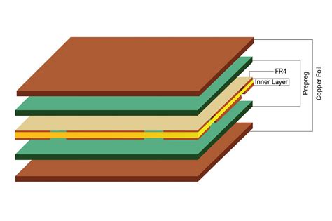
Lamination
Once the copper foil has been produced, it is laminated onto the insulating substrate material using heat and pressure. The lamination process typically involves stacking the copper foil and substrate material together, along with a layer of adhesive or prepreg (pre-impregnated) material, and then applying heat and pressure to bond the layers together.
Etching
After lamination, the excess copper is removed from the surface of the PCB through an etching process. This involves applying a photoresist layer to the copper surface, exposing it to UV light through a patterned mask, and then etching away the unwanted copper using a chemical solution. The resulting copper pattern defines the electrical connections on the PCB.
Surface Finishing
Once the etching process is complete, the PCB undergoes a surface finishing process to protect the exposed copper and improve its solderability. Common surface finishes include Hot Air Solder Leveling (HASL), Electroless Nickel Immersion Gold (ENIG), and Immersion Silver (IAg).

Attentions in PCB Copper Cladding
To ensure the optimal performance and reliability of PCBs, several key attentions need to be paid to the copper cladding during the manufacturing process and in use. These include:
Copper Thickness
The thickness of the copper cladding is a critical factor in determining the electrical and thermal performance of the PCB. Thicker copper layers offer lower resistance and better current-carrying capacity, but may be more challenging to etch accurately. Thinner copper layers, on the other hand, may be more susceptible to damage and signal loss. The appropriate copper thickness should be selected based on the specific requirements of the application.
| Copper Thickness (oz/ft²) | Thickness (µm) | Typical Applications |
|---|---|---|
| 0.5 | 17.5 | Low-power, high-density designs |
| 1 | 35 | General-purpose PCBs, moderate power requirements |
| 2 | 70 | High-power applications, automotive, industrial |
| 3 | 105 | Very high-power applications, power electronics |
Adhesion
The adhesion between the copper cladding and the insulating substrate is critical for the long-term reliability of the PCB. Poor adhesion can lead to delamination, cracking, and other failures, particularly when the PCB is subjected to thermal or mechanical stress. Proper surface preparation, lamination conditions, and material selection can help to ensure good adhesion and prevent these issues.
Etching Quality
The accuracy and uniformity of the etching process directly impact the quality of the electrical connections on the PCB. Over-etching or under-etching can lead to signal integrity issues, short circuits, or open connections. Proper control of the etching process parameters, such as the etchant concentration, temperature, and exposure time, is essential for achieving high-quality etching results.
Surface Finish Compatibility
The choice of surface finish can affect the compatibility of the PCB with the assembly process and the end-use environment. For example, some surface finishes may be more susceptible to oxidation or corrosion, while others may be more difficult to solder or may not be suitable for certain types of components. The surface finish should be selected based on the specific requirements of the application and the manufacturing process.
Thermal Management
The thermal conductivity of the copper cladding plays a key role in the thermal management of the PCB. Inadequate heat dissipation can lead to component overheating, reduced performance, and premature failure. The design of the PCB, including the copper thickness, trace width, and layout, should be optimized to ensure effective heat spreading and dissipation.

Frequently Asked Questions (FAQ)
-
What is the difference between ED and RA copper cladding?
ED (Electrodeposited) copper is produced by electroplating a thin layer of copper onto the insulating substrate, while RA (Rolled Annealed) copper is produced by rolling and annealing copper foil. RA copper offers better signal integrity and lower losses compared to ED copper, making it more suitable for high-frequency and high-speed applications. -
How does copper thickness affect PCB performance?
The thickness of the copper cladding impacts the electrical and thermal performance of the PCB. Thicker copper layers provide lower resistance and better current-carrying capacity, but may be more difficult to etch accurately. Thinner copper layers, on the other hand, may be more susceptible to damage and signal loss. The appropriate copper thickness should be selected based on the specific requirements of the application. -
What is the purpose of surface finishing in PCB copper cladding?
Surface finishing is applied to the exposed copper on the PCB to protect it from oxidation and corrosion, as well as to improve its solderability. Common surface finishes include HASL (Hot Air Solder Leveling), ENIG (Electroless Nickel Immersion Gold), and IAg (Immersion Silver). The choice of surface finish depends on the specific requirements of the application and the manufacturing process. -
How can adhesion problems in PCB copper cladding be prevented?
Adhesion problems between the copper cladding and the insulating substrate can be prevented by proper surface preparation, lamination conditions, and material selection. This includes ensuring that the surfaces are clean and free of contaminants, using appropriate lamination temperatures and pressures, and selecting compatible materials for the copper foil and substrate. -
Why is thermal management important in PCB copper cladding?
Thermal management is critical in PCB copper cladding because inadequate heat dissipation can lead to component overheating, reduced performance, and premature failure. The thermal conductivity of the copper cladding helps to spread and dissipate heat generated by electronic components on the PCB. Proper design of the PCB, including the copper thickness, trace width, and layout, is essential for ensuring effective thermal management.
Conclusion
PCB copper cladding is a critical element in the manufacturing of printed circuit boards, playing a vital role in the functionality, reliability, and performance of electronic devices. Understanding the types of copper cladding, manufacturing processes, and key attentions involved in PCB copper cladding is essential for ensuring the production of high-quality PCBs that meet the specific requirements of the application.
By selecting the appropriate copper thickness, ensuring good adhesion, optimizing the etching process, choosing compatible surface finishes, and considering thermal management, PCB manufacturers can produce boards that deliver optimal electrical performance, long-term reliability, and cost-effectiveness. As electronic devices continue to advance and become more complex, the importance of high-quality PCB copper cladding will only continue to grow, making it a crucial aspect of the electronics industry.


Leave a Reply