PCB Materials
The choice of materials used in PCB Construction plays a vital role in determining the board’s electrical, thermal, and mechanical properties. The most common materials used for PCB substrates include:
FR-4
FR-4 is a glass-reinforced epoxy laminate material widely used in PCB construction. It offers excellent electrical insulation, mechanical strength, and thermal stability, making it suitable for a wide range of applications.
High-Frequency Materials
For high-frequency applications, such as RF and microwave circuits, specialized materials like Rogers, Teflon, and ceramic-based laminates are used. These materials exhibit low dielectric loss and stable dielectric constant over a wide frequency range, ensuring optimal signal integrity.
Flexible Materials
Flexible PCBs are constructed using materials like polyimide or polyester, which allow the board to bend and flex without compromising its electrical functionality. These materials are ideal for applications that require conformity to irregular shapes or dynamic movement.
| Material | Dielectric Constant | Dissipation Factor | Thermal Conductivity (W/mK) |
|---|---|---|---|
| FR-4 | 4.5 | 0.02 | 0.3 |
| Rogers RO4350B | 3.48 | 0.0037 | 0.62 |
| Polyimide | 3.5 | 0.002 | 0.12 |
PCB Layering and Stacking
The number of layers and their arrangement in a PCB significantly impact its functionality and complexity. PCBs can be categorized based on the number of layers:
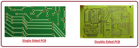
Single-Layer PCBs
Single-layer PCBs consist of a single conductive layer, typically copper, on one side of the substrate. They are the simplest and most cost-effective option for basic circuits with low component density.
Double-Layer PCBs
Double-layer PCBs have conductive layers on both sides of the substrate, allowing for more complex routing and higher component density compared to single-layer boards. The layers are interconnected using through-hole vias.
Multi-Layer PCBs
Multi-layer PCBs consist of three or more conductive layers, separated by insulating layers. They offer the highest level of complexity and density, enabling the routing of intricate circuits and the use of advanced packaging techniques like Ball Grid Arrays (BGA).
| PCB Type | Layers | Complexity | Applications |
|---|---|---|---|
| Single-Layer | 1 | Low | Simple circuits, low-density designs |
| Double-Layer | 2 | Medium | Moderate complexity, higher density |
| Multi-Layer | 3+ | High | Complex circuits, high-density designs |

PCB Trace Width and Spacing
The width and spacing of the conductive traces on a PCB are critical factors in ensuring proper signal integrity and preventing signal interference. The trace width determines the current-carrying capacity and resistance of the trace, while the spacing between traces affects the potential for crosstalk and electromagnetic interference (EMI).
Trace Width Calculation
The trace width is calculated based on several factors, including the required current-carrying capacity, the thickness of the copper layer, and the maximum allowable temperature rise. The IPC-2152 standard provides guidelines for determining the appropriate trace width based on these factors.
Clearance and Creepage
Clearance refers to the shortest distance between two conductive elements through air, while creepage is the shortest distance along the surface of the insulating material. Maintaining adequate clearance and creepage distances is essential to prevent electrical arcing and ensure the board’s reliability.
| Trace Width (mm) | Current Capacity (A) | Resistance (mΩ/cm) |
|---|---|---|
| 0.2 | 0.5 | 84 |
| 0.5 | 1.0 | 33 |
| 1.0 | 2.0 | 16 |

PCB Surface Finish
The surface finish of a PCB serves multiple purposes, including protecting the copper traces from oxidation, enhancing solderability, and improving the aesthetics of the board. Common surface finishes used in PCB construction include:
Hot Air Solder Leveling (HASL)
HASL is a widely used surface finish that involves immersing the PCB in molten solder and then removing the excess solder using hot air knives. It provides excellent solderability and is relatively inexpensive.
Electroless Nickel Immersion Gold (ENIG)
ENIG is a two-layer surface finish that consists of a layer of electroless nickel followed by a thin layer of immersion gold. It offers excellent corrosion resistance, good solderability, and is suitable for fine-pitch components.
Immersion Silver (IAg)
IAg is a single-layer surface finish that involves depositing a thin layer of silver onto the copper traces. It provides good solderability and is a cost-effective alternative to ENIG for some applications.
| Surface Finish | Thickness (µm) | Solderability | Shelf Life |
|---|---|---|---|
| HASL | 1-40 | Excellent | 12 months |
| ENIG | 3-8 (Ni), 0.05-0.15 (Au) | Excellent | 12 months |
| IAg | 0.1-0.3 | Good | 6 months |

PCB Component Placement and Routing
The placement of components on a PCB and the routing of traces between them are critical aspects of PCB design that impact the board’s functionality, signal integrity, and manufacturability.
Component Placement
Proper component placement involves considering factors such as thermal management, signal integrity, and manufacturability. Components should be placed in a way that minimizes the length of traces, reduces crosstalk, and facilitates efficient assembly processes.
Routing Techniques
PCB routing involves creating the conductive paths that connect the components on the board. Various routing techniques are used, depending on the complexity of the circuit and the design constraints:
- Manual Routing: Traces are manually drawn by the PCB designer, offering full control over the routing process but requiring significant time and effort.
- Auto-Routing: Automated routing algorithms are used to create the traces based on predefined rules and constraints, saving time and effort but potentially compromising optimality.
- Hybrid Routing: A combination of manual and auto-routing techniques is used, allowing the designer to manually route critical traces while using auto-routing for less critical ones.
PCB Testing and Inspection
To ensure the quality and reliability of PCBs, various testing and inspection techniques are employed throughout the manufacturing process.
Automated Optical Inspection (AOI)
AOI uses high-resolution cameras and image processing algorithms to automatically detect visual defects on the PCB, such as missing components, incorrect component placement, and solder bridging.
In-Circuit Testing (ICT)
ICT involves using a bed-of-nails fixture to make electrical contact with specific points on the PCB and verify the presence, orientation, and functionality of components, as well as the integrity of the interconnections.
Functional Testing
Functional testing involves powering up the PCB and verifying its operation under real-world conditions, ensuring that it meets the specified performance requirements.
Frequently Asked Questions (FAQ)
- What is the difference between a single-layer and a multi-layer PCB?
-
A single-layer PCB has conductive traces on only one side of the substrate, while a multi-layer PCB has three or more conductive layers separated by insulating layers, allowing for more complex routing and higher component density.
-
Why is the choice of surface finish important in PCB construction?
-
The surface finish protects the copper traces from oxidation, enhances solderability, and improves the aesthetics of the board. Different surface finishes offer varying levels of protection, solderability, and cost-effectiveness, making the choice dependent on the specific application requirements.
-
What factors determine the trace width on a PCB?
-
The trace width is determined by factors such as the required current-carrying capacity, the thickness of the copper layer, and the maximum allowable temperature rise. The IPC-2152 standard provides guidelines for calculating the appropriate trace width based on these factors.
-
How does PCB layering affect the complexity and functionality of the board?
-
The number of layers in a PCB directly influences its complexity and functionality. Single-layer PCBs are the simplest and most cost-effective option for basic circuits, while multi-layer PCBs offer the highest level of complexity and density, enabling the routing of intricate circuits and the use of advanced packaging techniques.
-
What are the common testing and inspection techniques used in PCB manufacturing?
- Common testing and inspection techniques include Automated Optical Inspection (AOI), which uses cameras and image processing to detect visual defects; In-Circuit Testing (ICT), which verifies the presence, orientation, and functionality of components using a bed-of-nails fixture; and Functional Testing, which involves powering up the PCB and verifying its operation under real-world conditions.
In conclusion, the construction of a Printed Circuit Board involves a complex interplay of various factors, including material selection, layering and stacking, trace width and spacing, surface finish, component placement and routing, and testing and inspection. By carefully considering these factors and making informed decisions throughout the design and manufacturing process, engineers can create PCBs that are reliable, functional, and cost-effective, enabling the development of increasingly sophisticated electronic devices and systems.


Leave a Reply