What is a PCB Via?
A Printed Circuit Board (PCB) via is a small hole drilled through a PCB that allows electrical connections between different layers of the board. Vias are essential components in multi-layer PCBs as they facilitate the routing of signals and power between layers, enabling more complex and compact designs.
Types of PCB Vias
There are several types of PCB vias, each with its own characteristics and applications:
-
Through Hole Via: These vias go through the entire thickness of the PCB, connecting all layers. They are the most common type of via and are typically used for components with through-hole pins.
-
Blind Via: Blind vias start from an outer layer and terminate at an inner layer, without going through the entire board. They are used to connect an outer layer to one or more inner layers.
-
Buried Via: Buried vias connect two or more inner layers without reaching either outer layer. They are used to create connections between inner layers, reducing the need for through hole vias and saving space on the outer layers.
-
Micro Via: Micro vias are small vias with diameters typically less than 150 microns. They are used in high-density interconnect (HDI) PCBs to create compact and intricate designs.
Factors Affecting PCB Via Size
Several factors influence the size of PCB vias:
PCB Thickness
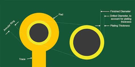
The thickness of the PCB is a crucial factor in determining the minimum via size. Thicker boards require larger vias to maintain the aspect ratio (the ratio of via depth to diameter) within acceptable limits. A high aspect ratio can lead to issues such as poor plating coverage and difficulty in cleaning the via.
Manufacturing Capabilities
The manufacturing capabilities of the PCB fabricator also play a role in determining the minimum via size. Advanced manufacturing processes and equipment enable the creation of smaller vias with tighter tolerances.
Via Plating
The plating process used for vias can affect their minimum size. Electroless plating, which involves depositing a thin layer of copper on the via walls, allows for smaller vias compared to electrolytic plating, which deposits a thicker layer of copper.
Current Carrying Capacity
The current carrying capacity of a via is determined by its cross-sectional area. Larger vias can handle higher currents without overheating or causing reliability issues. The required current carrying capacity of a via should be considered when selecting its size.

Standard PCB Via Sizes
The following table presents some standard PCB via sizes and their typical applications:
| Via Type | Diameter (mm) | Drill Size (mm) | Application |
|---|---|---|---|
| Through Hole | 0.8 – 1.0 | 0.3 – 0.5 | General purpose, through-hole components |
| Blind/Buried | 0.2 – 0.5 | 0.1 – 0.3 | High-density designs, inner layer connections |
| Micro Via | 0.1 – 0.15 | 0.05 – 0.1 | HDI PCBs, fine-pitch components |
It’s essential to consult with your PCB manufacturer to determine the minimum via sizes they can reliably produce based on their manufacturing capabilities and the specific requirements of your design.

Calculating PCB Via Size
To calculate the appropriate via size for your PCB design, consider the following factors:
-
PCB Thickness: Determine the thickness of your PCB and ensure that the aspect ratio of the via is within acceptable limits (typically 8:1 or less).
-
Current Carrying Capacity: Calculate the maximum current that will flow through the via and select a via size that can handle the current without overheating.
-
Manufacturing Capabilities: Consult with your PCB manufacturer to understand their minimum via size capabilities and any specific design rules they require.
-
Component Requirements: Consider the pin sizes and pitches of the components you plan to use and ensure that the via sizes are compatible.
Here’s an example calculation for determining the minimum via size based on PCB thickness and aspect ratio:
- PCB Thickness: 1.6 mm
- Maximum Aspect Ratio: 8:1
Minimum Via Diameter = PCB Thickness ÷ Maximum Aspect Ratio
Minimum Via Diameter = 1.6 mm ÷ 8 = 0.2 mm
In this example, the minimum via diameter is 0.2 mm, which would be suitable for a 1.6 mm thick PCB with an aspect ratio of 8:1.

Best Practices for PCB Via Design
To ensure optimal performance and reliability of your PCB vias, follow these best practices:
-
Minimize Via Count: Use the minimum number of vias necessary to route your signals effectively. Excessive vias can increase manufacturing costs and decrease reliability.
-
Place Vias Strategically: Position vias to minimize the length of signal paths and reduce the risk of signal integrity issues. Avoid placing vias in sensitive areas, such as under components or in high-speed signal paths.
-
Use Appropriate Via Size: Select via sizes that are compatible with your PCB thickness, manufacturing capabilities, and current carrying requirements. Avoid using vias that are too small, as they can be difficult to manufacture and may have limited current carrying capacity.
-
Consider Via-in-Pad: In some cases, placing vias directly in component pads can save space and simplify routing. However, ensure that your manufacturer can reliably produce via-in-pad structures and that the vias do not interfere with component soldering.
-
Follow Manufacturer Design Rules: Always adhere to the design rules and guidelines provided by your PCB manufacturer to ensure that your vias are manufacturable and reliable.
Frequently Asked Questions (FAQ)
-
Q: What is the smallest via size that can be manufactured?
A: The smallest via size depends on the manufacturing capabilities of your PCB fabricator. Some advanced manufacturers can produce micro vias with diameters as small as 0.1 mm (100 microns). -
Q: How does via size affect signal integrity?
A: Smaller vias can have higher inductance and resistance, which can affect signal integrity, particularly for high-speed signals. Larger vias generally have better signal integrity characteristics but may take up more space on the PCB. -
Q: Can vias be filled?
A: Yes, vias can be filled with a non-conductive material, such as epoxy, to improve the planarity of the PCB surface and facilitate the placement of components over vias. Filled vias can also help dissipate heat and improve the mechanical strength of the board. -
Q: What is via stacking?
A: Via stacking is a technique where vias are placed on top of each other in different layers of the PCB to create a continuous electrical connection. This method can save space on the board and simplify routing, but it requires precise alignment and may not be suitable for all designs. -
Q: How can I reduce the impact of vias on my PCB design?
A: To minimize the impact of vias on your PCB design, consider using blind and buried vias to reduce the number of through-hole vias, optimize via placement to minimize signal path lengths, and follow manufacturer design rules and best practices for via design.
By understanding the different types of PCB vias, factors affecting via size, and best practices for via design, you can create reliable and high-performance PCBs that meet your specific requirements. Always work closely with your PCB manufacturer to ensure that your via design is compatible with their manufacturing capabilities and design rules.


Leave a Reply