What are PCB Vias?
Printed Circuit Board (PCB) vias are small holes drilled through a PCB to electrically connect different layers of the board. Vias allow signals and power to pass vertically between the layers, enabling more complex routing and denser PCB designs.
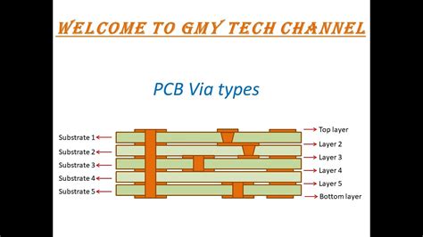
Types of PCB vias
There are several types of vias used in PCB design:
| Via Type | Description |
|---|---|
| Through-hole via | Passes through all layers of the PCB |
| Blind via | Connects an outer layer to an inner layer, but does not pass through the entire board |
| Buried via | Connects inner layers without reaching either outer layer |
| Microvia | A small via (typically less than 0.15mm in diameter) used for high-density interconnects |
The importance of vias in PCB design
Enabling multi-layer PCBs
Vias are essential for creating multi-layer PCBs. By allowing connections between layers, vias enable more complex routing and denser designs. This is particularly important for high-speed and high-frequency applications, where signal integrity and controlled impedance are critical.
Improving signal integrity
Properly designed vias can help maintain signal integrity in a PCB. By minimizing via length and optimizing via geometry, designers can reduce parasitic capacitance and inductance, which can degrade signal quality. Techniques such as via stitching and ground shielding can further improve signal integrity.
Facilitating heat dissipation
Vias can also play a role in thermal management of PCBs. Thermal vias, which are typically filled with a conductive material such as copper, can help transfer heat from components to other layers or to a heatsink. This is particularly important for high-power components that generate significant heat.

Via design considerations
Via size and aspect ratio
The size of a via is determined by its diameter and the thickness of the PCB. The aspect ratio of a via is the ratio of its length to its diameter. High aspect ratio vias can be challenging to manufacture reliably, so designers must consider the capabilities of their PCB fabricator when specifying via sizes.
Via placement and routing
The placement and routing of vias can have a significant impact on signal integrity and manufacturability. Vias should be placed to minimize signal path length and to avoid creating signal integrity issues such as stubs or impedance mismatches. Designers must also consider the clearance and spacing requirements for vias, as well as the potential for via-to-via or via-to-trace crosstalk.
Via filling and capping
Vias can be filled with a conductive material, typically copper, to improve thermal and electrical performance. Filled vias can also be capped with a non-conductive material to prevent solder from wicking into the via during assembly. The choice of filling and capping materials and processes can affect the reliability and cost of the PCB.

Advanced via technologies
High Density Interconnect (HDI) vias
HDI PCBs use small vias, typically microvias, to achieve very high routing density. HDI designs often use via-in-pad technology, where vias are placed directly in component pads to save space. HDI vias require precise manufacturing processes and can add cost to a PCB, but they enable the highest density designs.
Blind and buried vias
Blind and buried vias connect inner layers of a PCB without extending to the outer layers. These vias can be used to create more complex routing patterns and to reduce the size of a PCB. However, blind and buried vias add complexity and cost to PCB manufacturing, so they are typically only used when necessary.
Via-in-pad technology
Via-in-pad (VIP) technology places vias directly in the pads of surface-mount components. This saves space on the PCB and can improve signal integrity by reducing the length of the signal path. VIP requires careful design and manufacturing to ensure reliable solder joints and to prevent solder from wicking into the via.

PCB via manufacturing processes
Drilling
Vias are created by drilling holes through the PCB substrate. The choice of drilling method depends on the size and type of via, as well as the material of the substrate. Mechanical drilling is used for larger vias, while laser drilling is used for smaller vias and for materials that are difficult to drill mechanically.
Plating
After drilling, vias are plated with a conductive material, typically copper, to create an electrical connection between layers. The choice of plating method and material can affect the reliability and performance of the via. Electroless plating is often used for high-aspect-ratio vias, while electrolytic plating is used for larger vias and for filling vias.
Filling and capping
Vias can be filled with a conductive material to improve thermal and electrical performance, and capped with a non-conductive material to prevent solder wicking. The choice of filling and capping materials and processes depends on the requirements of the design and the capabilities of the PCB fabricator.
Testing and inspection of PCB vias
Continuity testing
Continuity testing verifies that vias are electrically connected as intended. This can be done with a simple multimeter or with automated test equipment (ATE). Continuity testing is typically performed before and after PCB assembly to ensure that vias have not been damaged during manufacturing or assembly.
Cross-sectioning
Cross-sectioning is a destructive testing method that involves cutting a PCB along a via and examining the cross-section under a microscope. This allows the via plating and geometry to be inspected for defects such as voids, cracks, or insufficient plating thickness. Cross-sectioning is typically performed on a sample basis rather than on every PCB.
Automated optical inspection (AOI)
AOI uses cameras and image processing software to inspect PCBs for defects, including via defects such as missing or misplaced vias. AOI can quickly inspect large numbers of PCBs and can detect defects that may be missed by manual inspection. However, AOI cannot detect all types of via defects and may require additional testing methods.
Common via defects and their causes
Insufficient plating thickness
Insufficient plating thickness can cause vias to have high resistance or to fail entirely. This can be caused by problems with the plating process, such as incorrect chemical concentrations or insufficient plating time. Insufficient plating can also be caused by contamination or by rough via walls that prevent uniform plating.
Voids and cracks
Voids and cracks in via plating can cause intermittent or complete failures. Voids can be caused by air bubbles or contaminants in the plating solution, while cracks can be caused by stress during manufacturing or assembly. Voids and cracks can be difficult to detect without destructive testing methods such as cross-sectioning.
Misplaced or missing vias
Misplaced or missing vias can cause open circuits or short circuits in a PCB. These defects can be caused by problems with the drilling process, such as drill bit wear or misalignment, or by problems with the artwork or CAM data used to generate the drill files. Misplaced or missing vias can usually be detected by automated optical inspection (AOI) or electrical testing.
Frequently Asked Questions (FAQ)
Q: What is the difference between a through-hole via and a blind via?
A: A through-hole via passes through all layers of the PCB, while a blind via connects an outer layer to an inner layer without passing through the entire board.
Q: Why are microvias used in HDI PCBs?
A: Microvias are used in HDI PCBs because their small size allows for higher routing density and more complex designs. Microvias are typically laser-drilled and can be placed directly in component pads to save space.
Q: How does via-in-pad technology improve signal integrity?
A: Via-in-pad technology places vias directly in the pads of surface-mount components, reducing the length of the signal path. This can improve signal integrity by reducing the inductance and capacitance of the signal path.
Q: What are some common causes of via defects?
A: Common causes of via defects include insufficient plating thickness, voids and cracks in the plating, and misplaced or missing vias. These defects can be caused by problems with the manufacturing process, such as incorrect plating chemistry or drill bit wear.
Q: How can via defects be detected?
A: Via defects can be detected through electrical testing methods such as continuity testing, as well as visual inspection methods such as automated optical inspection (AOI) and cross-sectioning. Each testing method has its own advantages and limitations, and a combination of methods may be necessary to fully characterize via quality.


Leave a Reply