Introduction to PCB Vias
A Printed Circuit Board (PCB) is a fundamental component in modern electronics, providing a platform for interconnecting electronic components. One crucial element in PCB design is the via, which allows for electrical connections between different layers of a multi-layer PCB. In this comprehensive article, we will explore what PCB Vias are, their types, and how to choose the right one for your project.
What is a PCB Via?
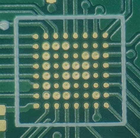
A PCB via is a small hole drilled through a printed circuit board to create an electrical connection between different layers of the board. Vias are typically plated with a conductive material, such as copper, to ensure reliable electrical conductivity. They enable designers to route traces on different layers, allowing for more compact and efficient PCB layouts.
The Importance of PCB Vias
PCB vias play a critical role in modern PCB design for several reasons:
- Space Savings: Vias allow designers to route traces on different layers, reducing the overall size of the PCB.
- Signal Integrity: Properly designed vias help maintain signal integrity by minimizing crosstalk and electromagnetic interference (EMI).
- Manufacturing Efficiency: Vias simplify the manufacturing process by allowing for automated drilling and plating.
Types of PCB Vias
There are several types of PCB vias, each with its own characteristics and applications. Understanding the differences between these types is essential for selecting the most suitable via for your project.
Through-Hole Vias
Through-hole vias are the most common type of via, consisting of a hole drilled through the entire thickness of the PCB. They are typically plated with copper to create an electrical connection between layers. Through-hole vias offer several advantages:
- Robustness: Through-hole vias provide a strong mechanical connection, making them suitable for high-stress applications.
- Simplified Assembly: Components with through-hole pins can be easily inserted and soldered to the PCB.
- High Current Capacity: The larger diameter of through-hole vias allows for higher current carrying capacity compared to other via types.
However, through-hole vias also have some limitations:
- Space Consumption: Through-hole vias require more space on the PCB, limiting the routing density.
- Manufacturing Cost: Drilling through-hole vias is more time-consuming and expensive compared to other via types.
Blind Vias
Blind vias are drilled from one side of the PCB and terminate at a specific inner layer, without penetrating through the entire board thickness. Blind vias offer several benefits:
- Space Savings: By not penetrating through the entire board, blind vias allow for higher routing density and more compact designs.
- Improved Signal Integrity: Blind vias minimize the stub effect, reducing signal reflections and improving signal integrity.
- Reduced Manufacturing Cost: Blind vias require fewer drilling steps compared to through-hole vias, reducing manufacturing time and cost.
However, blind vias also have some drawbacks:
- Limited Accessibility: Blind vias are not accessible from both sides of the PCB, which can complicate assembly and testing.
- Increased Design Complexity: Designing with blind vias requires careful planning and consideration of layer stackup and drilling depths.
Buried Vias
Buried vias are located entirely within the inner layers of a multi-layer PCB, without extending to either surface of the board. They provide several advantages:
- Improved Signal Integrity: Buried vias minimize the stub effect and reduce signal reflections, enhancing signal integrity.
- Space Savings: By being embedded within the inner layers, buried vias allow for higher routing density and more compact designs.
- Reduced EMI: Buried vias help minimize electromagnetic interference by containing signals within the inner layers of the PCB.
However, buried vias also have some limitations:
- Increased Manufacturing Complexity: Creating buried vias requires precise layer alignment and multiple lamination steps, increasing manufacturing complexity and cost.
- Limited Accessibility: Buried vias are not accessible from either side of the PCB, making testing and debugging more challenging.
Micro Vias
Micro vias are small-diameter vias, typically less than 150 microns (0.15 mm) in diameter. They are commonly used in high-density interconnect (HDI) PCBs and offer several benefits:
- Space Savings: The small size of micro vias allows for higher routing density and more compact designs.
- Improved Signal Integrity: Micro vias minimize the stub effect and reduce signal reflections, enhancing signal integrity.
- Reduced Layer Count: By using micro vias, designers can often reduce the number of layers required in a PCB, lowering manufacturing costs.
However, micro vias also have some challenges:
- Manufacturing Complexity: Creating micro vias requires specialized equipment and processes, such as laser drilling, which can increase manufacturing complexity and cost.
- Reliability Concerns: The small size of micro vias makes them more susceptible to thermal and mechanical stress, potentially affecting long-term reliability.

Choosing the Right PCB Via
Selecting the appropriate type of PCB via depends on several factors, including the specific requirements of your project, the available budget, and the manufacturing capabilities of your PCB fabricator. Consider the following guidelines when choosing the right PCB via:
- Space Constraints: If your design has limited space, consider using blind, buried, or micro vias to maximize routing density and minimize board size.
- Signal Integrity: For high-speed or sensitive signals, blind, buried, and micro vias can help improve signal integrity by reducing stub effects and signal reflections.
- Manufacturing Cost: Through-hole vias are generally the most cost-effective option, while blind, buried, and micro vias may increase manufacturing costs due to additional processing steps.
- Current Carrying Capacity: If your design requires high current carrying capacity, through-hole vias may be the best choice due to their larger diameter.
- Reliability: Consider the long-term reliability requirements of your project. Through-hole vias offer robust mechanical connections, while micro vias may be more susceptible to thermal and mechanical stress.
It’s essential to consult with your PCB fabricator to understand their capabilities and limitations regarding different via types. They can provide guidance on the most suitable via type for your specific project, taking into account manufacturability, cost, and reliability factors.

PCB Via Design Considerations
When designing PCB vias, several key factors should be considered to ensure optimal performance and manufacturability:
Via Size and Placement
The size and placement of vias can significantly impact the performance and manufacturability of your PCB. Consider the following guidelines:
- Via Diameter: Choose an appropriate via diameter based on the current carrying requirements and the available space on the PCB. Larger diameters allow for higher current capacity but consume more space.
- Via Pitch: Ensure adequate spacing between vias to prevent manufacturing issues, such as drill breakout or copper bridging. Consult with your PCB fabricator for recommended via pitch values.
- Via Placement: Place vias strategically to minimize the impact on signal integrity and to avoid interfering with component placement or routing channels.
Via Aspect Ratio
The via aspect ratio is the ratio of the via’s depth to its diameter. A higher aspect ratio can make drilling and plating more challenging, potentially affecting manufacturability and reliability. Consider the following:
- Manufacturability: Consult with your PCB fabricator to understand their capabilities and limitations regarding via aspect ratios. Some fabricators may have restrictions on the maximum aspect ratio they can reliably produce.
- Plating Uniformity: High aspect ratio vias can be more difficult to plate uniformly, potentially leading to inconsistent electrical connections or reduced reliability.
Via Stub and Back-Drilling
Via stubs, the unused portion of a via extending beyond the target layer, can cause signal reflections and degrade signal integrity, particularly in high-speed designs. Back-drilling is a process that removes the via stub to mitigate these issues. Consider the following:
- Signal Integrity: If your design includes high-speed signals, consider using blind or buried vias to minimize via stubs, or specify back-drilling to remove the stubs entirely.
- Manufacturing Cost: Back-drilling adds an additional processing step and can increase manufacturing costs. Weigh the benefits of improved signal integrity against the added cost.
Via-in-Pad Design
Via-in-pad design involves placing vias directly within component pads, allowing for more compact layouts and improved routing efficiency. However, this approach also presents some challenges:
- Soldermask Coverage: Ensure adequate soldermask coverage around the via to prevent solder from wicking into the via during reflow.
- Solder Joint Reliability: Via-in-pad designs can be more susceptible to solder joint cracking due to thermal stress. Consider using filled or capped vias to improve reliability.
- Manufacturing Compatibility: Confirm with your PCB fabricator and assembly provider that they can accommodate via-in-pad designs and any associated requirements, such as via filling or capping.
By carefully considering these design factors and working closely with your PCB fabricator, you can ensure that your PCB via design is optimized for performance, manufacturability, and reliability.

Frequently Asked Questions (FAQ)
-
What is the difference between a through-hole via and a blind via?
A through-hole via passes through the entire thickness of the PCB, while a blind via starts from one surface and terminates at an inner layer without reaching the opposite surface. -
Can I use micro vias in a standard PCB design?
Micro vias are typically used in high-density interconnect (HDI) PCB designs. While they can be used in standard PCB designs, they may increase manufacturing complexity and cost. Consult with your PCB fabricator to determine if micro vias are suitable for your specific project. -
How do I determine the appropriate via size for my PCB design?
The appropriate via size depends on several factors, including the current carrying requirements, available space on the PCB, and the manufacturing capabilities of your PCB fabricator. Consult with your fabricator to determine the optimal via size for your specific design. -
What is back-drilling, and when should I consider using it?
Back-drilling is a process that removes the unused portion of a via (via stub) to improve signal integrity in high-speed designs. Consider using back-drilling when your design includes high-speed signals and you want to minimize signal reflections caused by via stubs. -
Can I use via-in-pad design in my PCB?
Via-in-pad design can be used to create more compact layouts and improve routing efficiency. However, it’s essential to confirm with your PCB fabricator and assembly provider that they can accommodate via-in-pad designs and any associated requirements, such as via filling or capping.
Conclusion
PCB vias are essential components in modern PCB design, enabling efficient interconnections between layers and allowing for more compact layouts. Understanding the different types of vias, their characteristics, and their applications is crucial for selecting the most suitable via for your project. By considering factors such as space constraints, signal integrity, manufacturing cost, and reliability, you can make informed decisions when choosing PCB vias.
When designing with PCB vias, it’s essential to consider key factors such as via size and placement, aspect ratio, via stub and back-drilling, and via-in-pad design. By carefully addressing these design considerations and working closely with your PCB fabricator, you can ensure that your PCB via design is optimized for performance, manufacturability, and reliability.
As technology continues to advance, the importance of proper PCB via selection and design will only continue to grow. By staying informed about the latest developments in PCB via technology and best practices in via design, you can create PCBs that meet the ever-increasing demands of modern electronics.


Leave a Reply