Introduction to PCB Vias
A PCB via is a small hole drilled in a printed circuit board (PCB) that allows electrical connections to be made between different layers of the board. Vias are an essential component of multi-layer PCBs, enabling complex circuits to be routed in a compact space.
Types of PCB Vias
There are several types of PCB vias, each with its own characteristics and applications:
| Via Type | Description |
|---|---|
| Through Hole Via | Drilled through the entire board, connecting all layers |
| Blind Via | Connects an outer layer to an inner layer, but does not go through the entire board |
| Buried Via | Connects inner layers without reaching either outer layer |
| Microvia | A small via (typically less than 150 microns in diameter) used for high-density interconnects |
Through Hole Vias
Through hole vias are the most common type of via. They are drilled through the entire thickness of the PCB and metallized to create an electrical connection between all the layers. Through hole vias are reliable and easy to manufacture, but they consume a significant amount of board space and can limit the routing density.
Blind Vias
Blind vias connect an outer layer of the PCB to one or more inner layers, but do not go through the entire board. They are typically laser-drilled and can be smaller than through hole vias, allowing for higher routing density. However, blind vias are more expensive to manufacture and can be less reliable than through hole vias.
Buried Vias
Buried vias connect inner layers of the PCB without reaching either outer layer. They are created by drilling and metallizing the vias before laminating the inner layers together. Buried vias offer the highest routing density but are also the most expensive and complex to manufacture.
Microvias
Microvias are small vias, typically less than 150 microns in diameter, used for high-density interconnects. They can be either blind or buried and are often used in HDI (high-density interconnect) PCB designs. Microvias allow for very fine pitch components and can significantly reduce the size of the PCB.
PCB Via Manufacturing Process
The process of creating PCB vias involves several steps:
- Drilling: Holes are drilled into the PCB substrate using mechanical or laser drilling methods.
- Deburring: The drilled holes are cleaned to remove any debris or burrs.
- Metallization: The walls of the holes are coated with a conductive material, typically copper, to create an electrical connection.
- Plating: Additional copper is electroplated onto the metallized walls to increase the thickness and improve the conductivity.
Mechanical Drilling vs. Laser Drilling
PCB vias can be created using either mechanical drilling or laser drilling methods. Each method has its advantages and disadvantages:
| Method | Advantages | Disadvantages |
|---|---|---|
| Mechanical Drilling | – Lower cost – Suitable for larger vias – Reliable |
– Limited miniaturization – Slower than laser drilling – Requires tool changes |
| Laser Drilling | – Smaller via sizes – Faster than mechanical drilling – No tool wear |
– Higher cost – Limited material options – Requires precise control |
Via Metallization Techniques
There are several methods for metallizing PCB vias:
- Electroless Copper Plating: A thin layer of copper is deposited onto the via walls using a chemical process.
- Electrolytic Copper Plating: Additional copper is electroplated onto the electroless copper layer to increase the thickness and improve conductivity.
- Direct Metallization: A conductive polymer is deposited onto the via walls, followed by electroplating.

PCB Via Design Considerations
When designing PCBs with vias, several factors must be considered to ensure optimal performance and manufacturability:
Via Size and Aspect Ratio
The size of a via is determined by its diameter and the thickness of the PCB. The aspect ratio is the ratio of the via’s depth to its diameter. A higher aspect ratio makes it more difficult to metallize the via walls and can lead to reliability issues.
| PCB Thickness | Typical Via Diameter | Aspect Ratio |
|---|---|---|
| 0.062″ (1.6mm) | 0.020″ (0.5mm) | 3:1 |
| 0.093″ (2.4mm) | 0.025″ (0.6mm) | 3.7:1 |
| 0.125″ (3.2mm) | 0.030″ (0.8mm) | 4:1 |
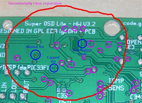
Via Placement and Spacing
The placement and spacing of vias are critical for ensuring signal integrity and avoiding manufacturing issues. Some guidelines for via placement include:
- Avoid placing vias under components, especially BGA (ball grid array) packages.
- Maintain adequate spacing between vias and other features, such as traces and pads.
- Use via-in-pad design for high-density layouts, but ensure the manufacturer can accommodate this.
- Minimize the number of vias in high-speed signal paths to reduce impedance discontinuities.
Via Shielding and Grounding
Vias can act as antennas, radiating electromagnetic interference (EMI) and causing signal integrity issues. To mitigate these problems, various via shielding and grounding techniques can be employed:
- Ground Vias: Place ground vias near signal vias to provide a low-impedance return path and reduce EMI.
- Shielding Vias: Surround signal vias with a ring of ground vias to create a Faraday cage and contain EMI.
- Stitching Vias: Use closely spaced vias to connect ground planes on different layers, reducing ground bounce and improving signal integrity.

PCB Via Reliability and Testing
The reliability of PCB vias is critical for the overall reliability of the circuit board. Several factors can affect via reliability:
- Thermal Stress: Temperature fluctuations can cause the via and surrounding material to expand and contract, leading to mechanical stress and potential failure.
- Mechanical Stress: Vibration, shock, and flexing of the PCB can cause via cracking or delamination.
- Chemical Contamination: Exposure to moisture, solvents, or other chemicals can degrade the via metallization and cause electrical failures.
To ensure via reliability, various testing methods are used:
- Microsectioning: The PCB is cross-sectioned, and the vias are examined under a microscope for defects or anomalies.
- Thermal Cycling: The PCB is subjected to repeated temperature cycles to simulate thermal stress and assess via integrity.
- Mechanical Testing: Vibration, shock, and flexure tests are performed to evaluate the mechanical robustness of the vias.
- Electrical Testing: Continuity, resistance, and insulation resistance tests are conducted to verify the electrical performance of the vias.

Future Trends in PCB Via Technology
As electronic devices continue to miniaturize and increase in complexity, PCB via technology must evolve to keep pace. Some emerging trends in via technology include:
- 3D Printing: Additive manufacturing techniques, such as direct ink writing (DIW), can create vias with unique geometries and materials, enabling new design possibilities.
- Via Filling: Completely filling vias with a conductive material can improve thermal and mechanical performance while reducing the risk of chemical contamination.
- Via Stacking: Stacking microvias on top of each other can create high-density interconnects without consuming additional board space.
- Embedded Components: Placing components inside via cavities can further increase packaging density and reduce the overall size of the PCB.
Frequently Asked Questions
1. What is the difference between a through hole via and a blind via?
A through hole via goes through the entire thickness of the PCB, connecting all layers. A blind via, on the other hand, connects an outer layer to one or more inner layers but does not go through the entire board.
2. What is the purpose of via shielding?
Via shielding is used to contain electromagnetic interference (EMI) generated by signal vias. By surrounding a signal via with a ring of ground vias, a Faraday cage is created, which helps to prevent EMI from affecting nearby components or traces.
3. What is the advantage of using microvias?
Microvias, which are typically less than 150 microns in diameter, allow for higher routing density and can accommodate very fine pitch components. This enables the design of smaller, more compact PCBs with increased functionality.
4. How can via reliability be improved?
Via reliability can be improved by:
– Optimizing via size and aspect ratio
– Using proper via shielding and grounding techniques
– Selecting appropriate materials and manufacturing processes
– Conducting thorough testing and quality control
5. What are some emerging trends in PCB via technology?
Some emerging trends in PCB via technology include 3D printing, via filling, via stacking, and embedded components. These advancements aim to increase packaging density, improve performance, and enable new design possibilities for future electronic devices.
Conclusion
PCB vias are a critical component of modern printed circuit boards, enabling complex circuits to be routed in compact spaces. By understanding the types of vias, manufacturing processes, design considerations, and reliability factors, PCB designers and manufacturers can create high-performance, reliable electronic devices. As technology continues to advance, innovations in via technology will play a crucial role in shaping the future of the electronics industry.


Leave a Reply