Table of Contents
- Introduction to Via-in-pad plating
- Benefits of Via-in-Pad Plating
- Challenges of Via-in-Pad Plating
- Applications of Via-in-Pad Plating
- Via-in-Pad Plating Manufacturing Process
- Design Considerations for Via-in-Pad Plating
- Frequently Asked Questions (FAQ)
- Conclusion
- References
Introduction to Via-in-Pad Plating
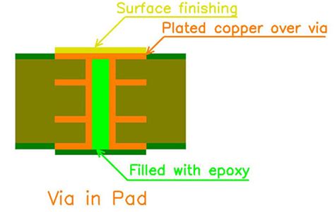
Via-in-pad plating is a PCB manufacturing technique that involves drilling and plating vias directly in the surface mount pads of a PCB. This technique differs from traditional PCB designs, where vias are typically placed outside the pads, requiring additional space and limiting the overall component density.
In a via-in-pad design, the via is an integral part of the pad itself, allowing for a more compact and efficient PCB layout. This integration is achieved by carefully controlling the via drilling and plating processes to ensure a smooth, even surface that can accommodate surface mount components.
Types of Via-in-Pad Plating
There are two main types of via-in-pad plating:
-
Filled Via-in-Pad: In this type, the via is completely filled with a conductive material, such as copper or a conductive epoxy, creating a smooth, flat surface. This method provides excellent mechanical strength and thermal conductivity.
-
Capped Via-in-Pad: In this type, the via is partially filled with a conductive material and then capped with a thin layer of copper or other conductive material. This method offers a compromise between the benefits of filled vias and the cost-effectiveness of traditional vias.

Benefits of Via-in-Pad Plating
Via-in-pad plating offers several significant benefits over traditional PCB designs:
-
Higher Density Interconnects: By placing vias directly in the pads, designers can achieve a more compact PCB layout, allowing for higher component density and smaller overall board sizes.
-
Improved Electrical Performance: Via-in-pad plating reduces the distance between components and their respective vias, minimizing signal path lengths and improving electrical performance. This is particularly important for high-speed and high-frequency applications.
-
Better Thermal Management: Filled via-in-pad designs offer excellent thermal conductivity, allowing for better heat dissipation from components to the PCB substrate and other layers.
-
Enhanced Mechanical Strength: Filled via-in-pad designs provide additional mechanical support to the pads, reducing the risk of pad cratering and improving the overall reliability of the PCB.
-
Space Savings: By eliminating the need for additional space around pads for via placement, via-in-pad plating enables more efficient use of PCB real estate, leading to cost savings and reduced board sizes.

Challenges of Via-in-Pad Plating
Despite its numerous benefits, via-in-pad plating also presents some challenges that must be addressed during the design and manufacturing processes:
-
Manufacturing Complexity: Via-in-pad plating requires precise control over the drilling and plating processes to ensure a smooth, even surface for component placement. This complexity can increase manufacturing costs and lead times.
-
Design Constraints: Via-in-pad designs must adhere to strict design rules, such as minimum via diameter, pad size, and copper thickness, to ensure manufacturability and reliability. Designers must carefully consider these constraints when creating via-in-pad PCB layouts.
-
Inspection and Testing: Due to the integrated nature of via-in-pad designs, inspection and testing can be more challenging compared to traditional PCB designs. Specialized equipment and techniques may be required to ensure the quality and reliability of via-in-pad PCBs.
-
Rework and Repair: Reworking or repairing via-in-pad PCBs can be more difficult than traditional designs, as the vias are an integral part of the pads. Special care must be taken to avoid damaging the pads or surrounding components during rework processes.

Applications of Via-in-Pad Plating
Via-in-pad plating is particularly well-suited for applications that require high density, high performance, and reliability:
-
Handheld and Portable Devices: Via-in-pad plating enables the creation of compact, lightweight PCBs for handheld and portable devices, such as smartphones, tablets, and wearables.
-
High-Speed Digital Devices: The improved electrical performance and reduced signal path lengths of via-in-pad designs make them ideal for high-speed digital applications, such as 5G communication devices, high-performance computing, and advanced driver assistance systems (ADAS).
-
RF and Microwave Devices: Via-in-pad plating is essential for RF and microwave devices, where signal integrity and low loss are critical. Applications include radar systems, satellite communication, and wireless infrastructure.
-
Aerospace and Defense: The enhanced mechanical strength and reliability of via-in-pad designs make them suitable for aerospace and defense applications, where PCBs must withstand harsh environmental conditions and high levels of stress.
-
Medical Devices: Via-in-pad plating enables the creation of compact, high-performance PCBs for medical devices, such as implantable devices, diagnostic equipment, and wearable health monitors.
Via-in-Pad Plating Manufacturing Process
The via-in-pad plating manufacturing process involves several key steps:
-
Drilling: High-precision drilling machines create the via holes directly in the pads of the PCB. The drilling process must be carefully controlled to ensure the correct via diameter and position.
-
Plating: The via holes are plated with a conductive material, typically copper, using electroplating or electroless plating techniques. The plating process must achieve a consistent thickness and uniformity to ensure reliable electrical connections.
-
Filling (Optional): For filled via-in-pad designs, the plated via holes are filled with a conductive material, such as copper or a conductive epoxy. The filling process must be carefully controlled to achieve a smooth, even surface.
-
Capping (Optional): For capped via-in-pad designs, a thin layer of copper or other conductive material is applied over the partially filled via to create a smooth surface for component placement.
-
Surface Finish: A surface finish, such as ENIG (Electroless Nickel Immersion Gold) or ENEPIG (Electroless Nickel Electroless Palladium Immersion Gold), is applied to the PCB to protect the exposed copper and enhance solderability.
Design Considerations for Via-in-Pad Plating
When designing PCBs with via-in-pad plating, several key factors must be considered:
-
Via Size and Placement: The via diameter and placement within the pad must be carefully chosen to ensure adequate electrical connection and mechanical strength. Designers must adhere to the manufacturer’s design rules and guidelines.
-
Pad Size and Shape: The pad size and shape must be designed to accommodate the via and provide sufficient space for component placement and soldering. Designers must consider the specific requirements of the chosen components and the PCB Assembly process.
-
Copper Thickness: The copper thickness of the pads and plated vias must be carefully selected to ensure reliable electrical connections and mechanical strength. Thicker copper can improve thermal management but may increase manufacturing costs.
-
Solder Mask Design: The solder mask design must be optimized for via-in-pad plating, ensuring adequate coverage of the via and surrounding area while leaving sufficient space for component placement and soldering.
-
Signal Integrity: Designers must carefully consider signal integrity requirements when creating via-in-pad PCB layouts, particularly for high-speed and high-frequency applications. Proper grounding, shielding, and impedance control techniques must be employed to minimize signal distortion and crosstalk.
Frequently Asked Questions (FAQ)
-
What is the difference between via-in-pad plating and traditional PCB Vias?
Via-in-pad plating involves placing vias directly in the surface mount pads of a PCB, while traditional PCB Vias are placed outside the pads. Via-in-pad plating allows for higher density interconnects, improved electrical performance, and better mechanical strength compared to traditional PCB designs. -
What are the main types of via-in-pad plating?
The two main types of via-in-pad plating are filled via-in-pad and capped via-in-pad. Filled via-in-pad designs involve completely filling the via with a conductive material, while capped via-in-pad designs partially fill the via and cap it with a thin layer of conductive material. -
What are the benefits of via-in-pad plating?
The benefits of via-in-pad plating include higher density interconnects, improved electrical performance, better thermal management, enhanced mechanical strength, and space savings compared to traditional PCB designs. -
What are the challenges associated with via-in-pad plating?
The challenges associated with via-in-pad plating include increased manufacturing complexity, strict design constraints, more challenging inspection and testing, and greater difficulty in rework and repair compared to traditional PCB designs. -
What applications are best suited for via-in-pad plating?
Via-in-pad plating is particularly well-suited for applications that require high density, high performance, and reliability, such as handheld and portable devices, high-speed digital devices, RF and microwave devices, aerospace and defense systems, and medical devices.
Conclusion
Via-in-pad plating is a powerful PCB manufacturing technique that offers numerous benefits over traditional PCB designs, including higher density interconnects, improved electrical performance, better thermal management, and enhanced mechanical strength. By placing vias directly in the surface mount pads of a PCB, via-in-pad plating enables the creation of compact, high-performance PCBs for a wide range of applications.
However, via-in-pad plating also presents challenges, such as increased manufacturing complexity, strict design constraints, and more difficult inspection and repair processes. Designers and manufacturers must carefully consider these factors when deciding whether to use via-in-pad plating for a particular project.
As technology continues to advance and the demand for smaller, faster, and more reliable electronic devices grows, via-in-pad plating will likely play an increasingly important role in PCB design and manufacturing. By understanding the fundamentals, benefits, and challenges of this innovative technique, designers and manufacturers can make informed decisions and create PCBs that meet the evolving needs of today’s electronic devices.
References
- IPC-7093: Design and Assembly Process Implementation for Bottom Termination Components, IPC International, Inc., 2011.
- Happy Holden, “Via-in-Pad: The Next Generation of High-Density Interconnects,” PCB007 Magazine, January 2021.
- “Via-in-Pad PCB design guidelines,” Sierra Circuits, accessed April 2023, https://www.protoexpress.com/blog/via-in-pad-pcb-design-guidelines/.
- “Via-in-Pad Plating: Benefits, Challenges, and Applications,” PCBCart, accessed April 2023, https://www.pcbcart.com/article/content/via-in-pad-plating.html.
- “Via-in-Pad PCB Manufacturing: Process, Design, and Considerations,” PCBWay, accessed April 2023, https://www.pcbway.com/blog/Engineering_Technical/Via_in_Pad_PCB_Manufacturing__Process__Design__and_Considerations.html.


Leave a Reply