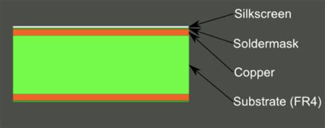
What is PCB Silkscreen?
PCB silkscreen, also known as legend or nomenclature, is the layer of text, symbols, and logos printed on the surface of a printed circuit board (PCB). The silkscreen layer is typically white, but other colors like black, yellow, or even custom colors can be used depending on the PCB’s design and purpose. The primary function of the silkscreen is to provide essential information about the board’s components, connectors, and other features, making it easier for engineers, technicians, and users to assemble, debug, and use the PCB.
The Importance of PCB Silkscreen
The silkscreen layer plays a crucial role in the overall functionality and usability of a PCB. Some of the key reasons why PCB silkscreen is essential include:
-
Component Identification: The silkscreen layer helps identify components on the PCB, such as resistors, capacitors, ICs, and connectors. This information is vital for assembly, troubleshooting, and repair processes.
-
Orientation Guidance: Silkscreen markings indicate the proper orientation of components, such as the pin-1 location of an IC or the polarity of a capacitor. This helps prevent assembly errors and ensures the correct functioning of the circuit.
-
User Instructions: The silkscreen can provide users with important instructions, such as the location of input/output connectors, switch positions, or LED indicators. This information makes it easier for users to interact with the PCB and understand its functionality.
-
Branding and Aesthetics: The silkscreen layer can include logos, product names, or other branding elements, enhancing the overall appearance and professional look of the PCB.
Key Considerations for PCB Silkscreen Design
When designing the silkscreen layer for a PCB, several factors should be taken into account to ensure optimal readability, clarity, and overall effectiveness.
Font Selection
Choosing the right font for your PCB silkscreen is essential for legibility and clarity. Some key points to consider when selecting a font include:
- Simplicity: Use simple, sans-serif fonts like Arial, Helvetica, or Verdana to ensure easy readability.
- Size: Ensure that the font size is large enough to be easily read. A minimum size of 0.8mm (0.032 inches) is recommended for most applications.
- Thickness: Use bold or thick fonts to improve visibility, especially on darker PCB substrates.
| Font | Minimum Size (mm) | Recommended Size (mm) |
|---|---|---|
| Arial | 0.8 | 1.0 |
| Helvetica | 0.8 | 1.0 |
| Verdana | 0.8 | 1.0 |
Placement and Spacing
The placement and spacing of silkscreen elements are crucial for readability and clarity. Some guidelines to follow include:
- Component Clearance: Ensure adequate space between the silkscreen and the components to avoid interfering with the assembly process. A minimum clearance of 0.5mm (0.020 inches) is recommended.
- Text Orientation: Orient text to be easily read from left to right or bottom to top. Avoid vertical or upside-down text whenever possible.
- Alignment: Align text and symbols with the components they refer to, making it easy to associate the silkscreen information with the corresponding elements on the PCB.
Symbols and Logos
In addition to text, the silkscreen layer can include various symbols and logos to convey information or enhance the PCB’s appearance. When incorporating symbols and logos, consider the following:
- Standardization: Use standard symbols whenever possible, such as those for ground, power, or antenna connections. This helps ensure consistency and familiarity for users.
- Clarity: Ensure that symbols and logos are clear, simple, and easily recognizable. Avoid overly complex or detailed designs that may not translate well to the silkscreen layer.
- Size: Keep symbols and logos at an appropriate size to maintain legibility and avoid overcrowding the PCB layout.

Avoiding Common PCB Silkscreen Mistakes
To ensure the effectiveness and quality of your PCB silkscreen, it’s important to avoid common mistakes that can lead to readability issues or assembly problems.
Overlapping with Solder Pads
One of the most common mistakes in PCB silkscreen design is allowing the silkscreen to overlap with solder pads. This can lead to several issues, including:
- Solder Mask Clearance: If the silkscreen overlaps with the solder mask opening around a pad, it can interfere with the soldering process and cause poor connections.
- Legibility: Overlapping silkscreen can obscure the solder pad, making it difficult to locate and solder components accurately.
To avoid these issues, always maintain a minimum clearance of 0.2mm (0.008 inches) between the silkscreen and solder pads.
Inconsistent or Confusing Naming Conventions
Inconsistent or confusing naming conventions can lead to assembly errors and difficulty in troubleshooting. To prevent these issues:
- Use Descriptive Names: Use clear, descriptive names for components, such as “LED1” or “BUTTON_PWR” instead of generic labels like “D1” or “SW1”.
- Maintain Consistency: Ensure that naming conventions are consistent throughout the PCB design, including schematic, layout, and silkscreen layers.
- Follow Industry Standards: Adhere to industry-standard naming conventions when applicable, such as those for power supply voltages (e.g., VCC, VDD, GND) or connectors (e.g., USB, HDMI).
Insufficient Contrast
Insufficient contrast between the silkscreen and the PCB substrate can make the silkscreen difficult to read, particularly in low-light conditions or when the PCB is populated with components. To ensure adequate contrast:
- Choose Appropriate Colors: Select silkscreen colors that provide good contrast against the PCB substrate. White silkscreen on a dark substrate or black silkscreen on a light substrate generally offers the best readability.
- Consider Lighting Conditions: If the PCB will be used in low-light environments, consider using a lighter silkscreen color or a reflective ink to enhance visibility.

FAQs
- What is the recommended minimum font size for PCB silkscreen?
-
The recommended minimum font size for PCB silkscreen is 0.8mm (0.032 inches) to ensure legibility.
-
How much clearance should be maintained between the silkscreen and components?
-
A minimum clearance of 0.5mm (0.020 inches) should be maintained between the silkscreen and components to avoid interfering with the assembly process.
-
Can I use custom colors for my PCB silkscreen?
-
Yes, custom colors can be used for PCB silkscreen, but it’s important to ensure that the chosen color provides adequate contrast against the PCB substrate for optimal readability.
-
What should I do if my logo is too complex for the silkscreen layer?
-
If your logo is too complex for the silkscreen layer, consider simplifying the design or using an alternative method, such as a sticker or label, to include the logo on the PCB.
-
How can I ensure consistency in naming conventions across my PCB design?
- To ensure consistency in naming conventions, establish a clear set of guidelines for component and feature naming early in the design process, and communicate these guidelines to all team members involved in the project. Additionally, use automated tools, such as design rule checks (DRC), to verify naming consistency throughout the design.
By following these guidelines and best practices for PCB silkscreen design, you can create clear, informative, and visually appealing PCBs that are easier to assemble, debug, and use. Remember to prioritize legibility, consistency, and clarity throughout the design process to ensure the best possible outcome for your PCB project.


Leave a Reply