Introduction to Multi-layer Boards
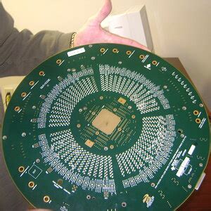
Multi-layer boards, also known as multilayer printed circuit boards (PCBs), are a type of PCB that consists of three or more conductive copper layers laminated together with insulating material between each layer. These boards are designed to accommodate complex electronic circuits and provide a higher density of interconnections compared to single or double-layer boards.
Advantages of Multi-layer Boards
- Increased circuit density
- Improved signal integrity
- Reduced electromagnetic interference (EMI)
- Better power distribution
- Smaller form factor
Construction of Multi-layer Boards
Layers in a Multi-layer Board
A multi-layer board typically consists of the following layers:
- Top layer (component side)
- Inner layers (signal layers)
- Power and ground planes
- Bottom layer (solder side)
The number of layers in a multi-layer board can vary depending on the complexity of the circuit and the application requirements. Common layer counts include 4, 6, 8, 10, 12, and even up to 50 layers or more for highly complex designs.
Materials Used in Multi-layer Boards
- Copper foil: Used for the conductive layers
- Prepreg: A pre-impregnated fiberglass material used as an insulator between layers
- Core: A fully cured fiberglass material used as a base for the inner layers
- Solder mask: A protective coating applied to the outer layers to prevent short circuits and provide insulation
- Silkscreen: A printed layer used for component labeling and identification
Manufacturing Process of Multi-layer Boards
The manufacturing process of multi-layer boards involves several steps:
- Inner layer fabrication: Copper foil is laminated onto a core material, and the desired circuit pattern is etched.
- Layer stacking: The inner layers are aligned and stacked with prepreg material between each layer.
- Lamination: The stacked layers are subjected to high pressure and temperature to bond them together.
- Drilling: Holes are drilled through the laminated board for component placement and interconnections.
- Plating: The drilled holes are plated with copper to establish electrical connections between layers.
- Outer layer fabrication: The top and bottom layers are laminated onto the board, and the circuit patterns are etched.
- Solder mask application: A solder mask is applied to the outer layers for protection and insulation.
- Silkscreen printing: Component labels and identifications are printed onto the board.
- Surface finish application: A surface finish, such as HASL, ENIG, or OSP, is applied to the exposed copper areas for solderability and protection.
Design Considerations for Multi-layer Boards
Signal Integrity
Maintaining signal integrity is crucial in multi-layer board design. Factors that can affect signal integrity include:
- Crosstalk: Unwanted coupling between adjacent traces
- Impedance: The resistance to the flow of alternating current in a circuit
- Reflections: Signal reflections caused by impedance mismatches
- Skew: Difference in propagation delay between signals
To minimize these issues, designers should consider the following:
- Proper trace routing and spacing
- Controlled impedance design
- Termination techniques
- Differential signaling
Power Distribution
Efficient power distribution is essential for the proper functioning of electronic circuits. In multi-layer boards, power and ground planes are used to distribute power evenly across the board. Designers should consider the following:
- Proper placement of power and ground planes
- Adequate copper thickness for current carrying capacity
- Decoupling capacitors for noise reduction
- Via placement for low-impedance connections
Thermal Management
As electronic components generate heat during operation, thermal management is an important consideration in multi-layer board design. Techniques for managing heat include:
- Proper component placement
- Thermal vias for heat dissipation
- Heat sinks and cooling solutions
- Thermally conductive materials
Manufacturability
Designing multi-layer boards with manufacturability in mind can help reduce costs and improve yield. Designers should consider the following:
- Design for manufacturing (DFM) guidelines
- Minimum feature sizes and spacing
- Hole and via sizes and placement
- Solder mask and silkscreen requirements

Applications of Multi-layer Boards
Multi-layer boards find applications in various industries and products, including:
- Consumer electronics (smartphones, tablets, laptops)
- Automotive electronics (infotainment systems, ECUs)
- Medical devices (diagnostic equipment, implantable devices)
- Industrial automation (PLCs, control systems)
- Aerospace and defense (avionics, satellite systems)
- Telecommunications (routers, switches, base stations)
Advantages of Using Multi-layer Boards
Miniaturization
Multi-layer boards enable the miniaturization of electronic devices by allowing for higher component density and more compact packaging. This is particularly important in applications where space is limited, such as smartphones, wearables, and implantable medical devices.
Improved Performance
The use of multi-layer boards can improve the overall performance of electronic systems by:
- Reducing signal interference and crosstalk
- Improving power distribution and regulation
- Minimizing EMI and RFI
- Enhancing thermal management
These improvements lead to more reliable and efficient electronic devices.
Cost Reduction
Although the initial design and fabrication costs of multi-layer boards may be higher compared to single or double-layer boards, they can lead to overall cost savings in the long run. This is achieved through:
- Reduced assembly time and costs
- Improved yield and reliability
- Smaller form factors, leading to reduced material costs
- Simplified inventory management
Challenges in Multi-layer Board Design and Manufacturing
Design Complexity
Designing multi-layer boards is more complex than single or double-layer boards due to the increased number of layers and the need to consider signal integrity, power distribution, and thermal management. This complexity requires skilled designers and advanced design tools.
Manufacturing Challenges
Manufacturing multi-layer boards involves several critical steps, each of which can introduce potential issues. Some of the challenges include:
- Layer registration and alignment
- Lamination defects (delamination, voids)
- Drilling and plating issues
- Solder mask and silkscreen defects
Proper process control and quality assurance measures are essential to minimize these issues.
Testing and Inspection
Testing and inspecting multi-layer boards is more challenging compared to single or double-layer boards due to the inability to directly access inner layers. Special techniques, such as X-ray inspection and microsectioning, may be required to verify the integrity of internal connections and structures.
Future Trends in Multi-layer Board Technology
High-Density Interconnect (HDI)
HDI technology involves the use of smaller vias, finer pitch components, and thinner dielectric materials to achieve even higher circuit densities. This technology enables the design of more compact and advanced electronic devices.
Embedded Components
Embedding active and passive components within the layers of a multi-layer board can further increase circuit density and reduce the overall size of electronic devices. This technology is particularly useful in applications where space is at a premium, such as implantable medical devices.
3D Printing
The use of 3D printing technologies, such as additive manufacturing and inkjet printing, is emerging as a potential alternative to traditional multi-layer board manufacturing methods. These technologies offer the potential for rapid prototyping, customization, and the creation of complex, three-dimensional structures.
Frequently Asked Questions (FAQ)
-
What is the difference between a multi-layer board and a single or double-layer board?
A multi-layer board consists of three or more conductive layers, while single and double-layer boards have one and two conductive layers, respectively. Multi-layer boards offer higher circuit density, improved signal integrity, and better power distribution compared to single or double-layer boards. -
How many layers can a multi-layer board have?
The number of layers in a multi-layer board can vary depending on the complexity of the circuit and the application requirements. Common layer counts include 4, 6, 8, 10, 12, and even up to 50 layers or more for highly complex designs. -
What materials are used in the construction of multi-layer boards?
Multi-layer boards are constructed using a combination of materials, including copper foil for the conductive layers, prepreg and core materials for insulation, solder mask for protection, and silkscreen for labeling. -
What are some of the key design considerations for multi-layer boards?
Key design considerations for multi-layer boards include signal integrity, power distribution, thermal management, and manufacturability. Designers must consider factors such as trace routing, impedance control, decoupling, heat dissipation, and design for manufacturing guidelines. -
What are some of the applications of multi-layer boards?
Multi-layer boards find applications in various industries, including consumer electronics, automotive electronics, medical devices, industrial automation, aerospace and defense, and telecommunications. They are used in products such as smartphones, laptops, infotainment systems, diagnostic equipment, control systems, avionics, and networking equipment.
Conclusion
Multi-layer boards are essential components in modern electronic devices, offering high circuit density, improved performance, and reduced form factors. The design and manufacturing of multi-layer boards involve several critical considerations, such as signal integrity, power distribution, thermal management, and manufacturability.
As electronic devices continue to evolve and become more complex, the demand for advanced multi-layer board technologies, such as HDI and embedded components, is expected to grow. Additionally, emerging technologies like 3D printing may offer new possibilities for the design and fabrication of multi-layer boards.
Understanding the fundamentals of multi-layer boards, their construction, design considerations, and applications is crucial for engineers, designers, and manufacturers involved in the development of electronic products. By staying informed about the latest trends and technologies in multi-layer board design and manufacturing, professionals can create innovative, reliable, and cost-effective electronic solutions.
Leave a Reply