What is a PCB Pad?
A PCB pad, also known as a solder pad or a surface mount pad, is a key component in printed circuit board (PCB) design. It is a flat, conductive area on the surface of a PCB where electronic components are soldered. PCB pads provide a reliable electrical and mechanical connection between the components and the copper traces on the board.
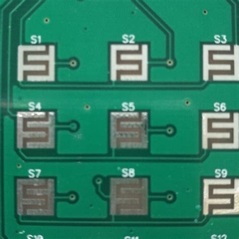
PCB pads come in various shapes and sizes, depending on the type of component they are designed to accommodate. The most common shapes are rectangular, oval, and circular. The size of the pad is determined by the size of the component lead or terminal that will be soldered to it.
The Importance of PCB Pads
PCB pads play a crucial role in ensuring the proper functioning and reliability of electronic devices. They serve several important purposes:
-
Electrical connection: PCB pads provide a conductive surface for soldering components to the board, allowing electrical current to flow between the component and the copper traces.
-
Mechanical support: Pads help to mechanically secure components to the PCB, preventing them from moving or becoming disconnected due to vibration or physical stress.
-
Heat dissipation: Pads also act as a heat sink, helping to dissipate heat generated by components during operation.
-
Manufacturing process: Pads are essential for the automated assembly process, as they provide a target for pick-and-place machines and soldering equipment.

Types of PCB Pads
There are several types of PCB pads, each designed for specific components and applications:
SMD Pads
Surface Mount Device (SMD) pads are designed for surface mount components, such as resistors, capacitors, and integrated circuits. These pads are typically smaller than through-hole pads and are located on the surface of the PCB.
SMD pads come in various sizes and shapes, depending on the component package. Some common SMD pad types include:
- Rectangular pads for chip resistors and capacitors
- Gull-wing pads for small-outline integrated circuits (SOIC)
- J-lead pads for plastic leaded chip carriers (PLCC)
- Quad flat pack (QFP) pads for QFP components
Through-Hole Pads
Through-hole pads are designed for components with leads that pass through holes in the PCB. These pads are typically larger than SMD pads and are located on both sides of the board.
Through-hole pads are often used for larger components or those that require a stronger mechanical connection, such as connectors, switches, and power transistors.
Solder Mask Defined (SMD) Pads
Solder Mask Defined (SMD) pads are a type of SMD pad where the solder mask opening is smaller than the copper pad itself. This design helps to control the amount of solder applied to the pad during the soldering process, reducing the risk of bridging between adjacent pads.
Non-Solder Mask Defined (NSMD) Pads
Non-Solder Mask Defined (NSMD) pads are SMD pads where the solder mask opening is larger than the copper pad. This design allows for more solder to be applied to the pad, creating a stronger mechanical connection. However, NSMD pads can be more prone to solder bridging if not properly designed.

PCB Pad Design Considerations
When designing PCB pads, several factors must be considered to ensure optimal performance and reliability:
Pad Size and Shape
The size and shape of a PCB pad should be determined by the size and type of component it will accommodate. Pads that are too small may result in weak solder joints or difficulty during the assembly process. Pads that are too large may lead to solder bridging or increased parasitic capacitance.
The table below shows some common SMD pad sizes for various component packages:
| Component Package | Pad Length (mm) | Pad Width (mm) |
|---|---|---|
| 0402 | 0.5 | 0.5 |
| 0603 | 0.8 | 0.8 |
| 0805 | 1.0 | 1.2 |
| 1206 | 1.6 | 1.6 |
| SOIC-8 | 2.0 | 0.6 |
| TQFP-44 | 0.8 | 0.4 |
Pad Spacing
The spacing between PCB pads is critical to prevent solder bridging and ensure proper insulation between components. The minimum pad spacing is determined by the PCB manufacturing capabilities and the soldering process used.
For example, a typical minimum pad spacing for a standard PCB with a solder mask is 0.2 mm. However, for fine-pitch components or high-density designs, smaller pad spacing may be required, which can increase manufacturing costs.
Solder Mask Opening
The solder mask opening is the area around the copper pad that is exposed for soldering. The size of the solder mask opening affects the amount of solder applied to the pad and the strength of the solder joint.
For SMD pads, the solder mask opening is typically designed to be slightly smaller than the copper pad (Solder Mask Defined) to control the amount of solder applied. For NSMD pads, the solder mask opening is larger than the copper pad, allowing for more solder to be applied.
Thermal Relief
Thermal relief is a design technique used to improve the solderability of PCB pads connected to large copper areas, such as ground or power planes. Thermal relief pads have a series of narrow spokes or a “web” pattern that connects the pad to the larger copper area. This design reduces the heat sinking effect of the large copper area, allowing the pad to reach the necessary temperature for soldering.

PCB Pad Materials
PCB pads are typically made from copper, which is an excellent conductor of electricity and heat. The copper pads are plated with a thin layer of another metal to improve solderability and protect against oxidation. Some common pad plating materials include:
-
Tin-Lead (SnPb): A traditional plating material that provides good solderability and reliability. However, due to environmental concerns, lead-based plating is being phased out in favor of lead-free alternatives.
-
Immersion Silver (IAg): A lead-free plating option that offers excellent solderability and a flat surface finish. IAg is compatible with both lead-free and tin-lead soldering processes.
-
Electroless Nickel Immersion Gold (ENIG): A two-layer plating process that consists of a nickel underlayer and a thin gold top layer. ENIG provides excellent solderability, durability, and a flat surface finish.
-
Organic Solderability Preservative (OSP): A lead-free, organic coating that protects the copper pads from oxidation and improves solderability. OSP is a cost-effective alternative to metal plating but may have a shorter shelf life.
PCB Pad Soldering Techniques
Soldering is the process of joining two metal surfaces by melting a filler metal (solder) between them. In PCB assembly, soldering is used to create electrical and mechanical connections between components and the PCB pads.
There are two main soldering techniques used in PCB assembly:
Wave Soldering
Wave soldering is a process where the PCB is passed over a wave of molten solder. This technique is primarily used for through-hole components, as the solder wave can fill the holes and create a strong mechanical connection.
Reflow Soldering
Reflow soldering is a process where a solder paste (a mixture of tiny solder balls and flux) is applied to the PCB pads, and the components are placed on top. The PCB is then heated in a reflow oven, melting the solder paste and creating a strong bond between the components and the pads.
Reflow soldering is the primary method used for surface mount components, as it allows for precise control over the amount of solder applied and can accommodate high-density designs.
Frequently Asked Questions (FAQ)
- What is the difference between SMD and NSMD pads?
-
SMD (Solder Mask Defined) pads have a solder mask opening that is smaller than the copper pad, while NSMD (Non-Solder Mask Defined) pads have a solder mask opening that is larger than the copper pad. SMD pads help control the amount of solder applied, while NSMD pads allow for more solder and a stronger mechanical connection.
-
Why are thermal relief pads used?
-
Thermal relief pads are used to improve the solderability of pads connected to large copper areas, such as ground or power planes. The thermal relief design reduces the heat sinking effect of the large copper area, allowing the pad to reach the necessary temperature for soldering.
-
What is the purpose of pad plating?
-
Pad plating is a thin layer of metal applied to the copper pads to improve solderability, protect against oxidation, and enhance the durability of the pads. Common plating materials include tin-lead, immersion silver, ENIG, and OSP.
-
How do I choose the right pad size for a component?
-
The pad size should be determined by the size and type of component it will accommodate. Refer to the component manufacturer’s datasheet for recommended pad dimensions. Pads that are too small may result in weak solder joints, while pads that are too large may lead to solder bridging or increased parasitic capacitance.
-
What is the minimum pad spacing for a standard PCB?
- The minimum pad spacing for a standard PCB with a solder mask is typically 0.2 mm. However, for fine-pitch components or high-density designs, smaller pad spacing may be required, which can increase manufacturing costs. Always consult with your PCB manufacturer for their specific capabilities and recommendations.
Conclusion
PCB pads are essential components in printed circuit board design, providing electrical, mechanical, and thermal connections between components and the board. Understanding the different types of pads, design considerations, materials, and soldering techniques is crucial for creating reliable and high-performance electronic devices.
By following best practices in pad design, such as choosing the appropriate size, shape, spacing, and plating, designers can ensure optimal functionality and manufacturability of their PCBs. As electronic devices continue to become smaller and more complex, the importance of proper PCB pad design will only continue to grow.


Leave a Reply