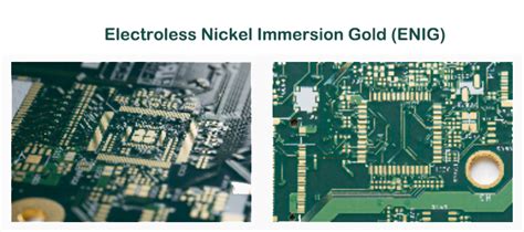
What is ENIG?
ENIG is a two-layer metallic coating that is applied to the copper pads and through-holes of a PCB. The first layer consists of electroless nickel, which is deposited onto the copper surface through an auto-catalytic chemical reaction. This nickel layer provides a barrier between the copper and the environment, preventing oxidation and ensuring good solderability. The second layer is a thin immersion gold coating that is deposited onto the nickel surface. The gold layer serves as a protective finish, preventing the nickel from oxidizing and providing a surface that is easy to solder.
Advantages of ENIG
- Excellent solderability
- ENIG provides a flat, solderable surface that ensures reliable and consistent solder joints.
-
The gold layer prevents oxidation of the underlying nickel, maintaining solderability over time.
-
Durability
- The nickel layer acts as a barrier, protecting the copper from corrosion and wear.
-
ENIG is resistant to multiple reflow cycles and has a long shelf life.
-
Flatness
- ENIG produces a flat surface finish, which is essential for fine-pitch components and high-density PCB designs.
-
The flat surface enables better contact between the component leads and the PCB Pads, improving electrical performance.
-
Wire Bonding compatibility
-
The gold surface of ENIG is suitable for wire bonding, making it a good choice for applications that require this interconnection method.
-
RoHS compliance
- ENIG is a lead-free and RoHS-compliant surface finish, meeting environmental regulations.
Disadvantages of ENIG
- Higher cost
- ENIG is more expensive compared to other surface finishes like HASL (Hot Air Solder Leveling) or OSP (Organic Solderability Preservative).
-
The cost is primarily due to the use of gold in the process.
-
Black pad syndrome
- In some cases, ENIG can suffer from “black pad syndrome,” where the nickel layer becomes brittle and separates from the copper surface.
-
This issue can lead to poor solderability and reduced reliability of the solder joints.
-
Difficulty in inspection
- The gold layer in ENIG can make visual inspection of solder joints more challenging, as it may obscure some defects.
ENIG Process
The ENIG process involves several steps to achieve the desired surface finish. These steps are:
- Cleaning
- The PCB is thoroughly cleaned to remove any contaminants or oxides from the copper surface.
-
This step ensures good adhesion of the subsequent layers.
-
Microetching
- The copper surface is microetched to create a slightly rough surface profile.
-
This roughness improves the mechanical bonding between the copper and the electroless nickel layer.
-
Electroless nickel plating
- The PCB is immersed in an electroless nickel plating bath, where the nickel is deposited onto the copper surface through an auto-catalytic chemical reaction.
-
The nickel layer is typically 3-6 μm thick and provides a barrier between the copper and the environment.
-
Immersion gold plating
- After the nickel plating, the PCB is immersed in an immersion gold plating bath.
- The gold layer is deposited onto the nickel surface through a displacement reaction, replacing some of the nickel atoms with gold atoms.
-
The gold layer is typically 0.05-0.2 μm thick and serves as a protective finish.
-
Drying
- The PCB is rinsed and dried after the gold plating process.

ENIG vs. Other Surface Finishes
ENIG is one of several surface finishing options available for PCBs. Some of the other common surface finishes include:
- HASL (Hot Air Solder Leveling)
- HASL is a low-cost surface finish that involves dipping the PCB in molten solder and then using hot air to remove the excess solder.
-
It provides good solderability but may result in an uneven surface and is not suitable for fine-pitch components.
-
OSP (Organic Solderability Preservative)
- OSP is a thin organic coating that is applied to the copper surface to prevent oxidation.
-
It is a low-cost option but has a limited shelf life and may not be suitable for multiple reflow cycles.
-
Immersion Silver
- Immersion silver is a single-layer metallic coating that is applied to the copper surface through a displacement reaction.
-
It offers good solderability and is less expensive than ENIG, but it may tarnish over time and has a shorter shelf life.
-
Immersion Tin
- Immersion tin is another single-layer metallic coating that is applied to the copper surface through a displacement reaction.
- It provides good solderability and is less expensive than ENIG, but it may form whiskers over time, which can cause short circuits.
The table below compares the properties of ENIG with other common surface finishes:
| Property | ENIG | HASL | OSP | Immersion Silver | Immersion Tin |
|---|---|---|---|---|---|
| Solderability | Excellent | Good | Good | Good | Good |
| Flatness | Excellent | Poor | Excellent | Good | Good |
| Durability | Excellent | Good | Poor | Fair | Fair |
| Wire Bonding | Yes | No | No | Yes | No |
| Shelf Life | Long | Long | Short | Medium | Medium |
| Cost | High | Low | Low | Medium | Medium |

Applications of ENIG
ENIG is widely used in various applications due to its excellent solderability, flatness, and durability. Some of the common applications include:
- High-density PCBs
-
ENIG’s flat surface finish makes it suitable for high-density PCB designs with fine-pitch components.
-
Automotive electronics
-
The durability and reliability of ENIG make it a good choice for automotive electronics that are exposed to harsh environments.
-
Aerospace and defense
-
ENIG’s long shelf life and resistance to multiple reflow cycles are beneficial for aerospace and defense applications.
-
Medical devices
-
The biocompatibility and durability of ENIG are advantageous for medical device applications.
-
Consumer electronics
- ENIG’s excellent solderability and compatibility with various components make it a popular choice for consumer electronics.

FAQ
- What does ENIG stand for?
-
ENIG stands for Electroless Nickel Immersion Gold. It is a surface finishing technique used in the manufacturing of printed circuit boards (PCBs).
-
What are the advantages of ENIG?
-
ENIG offers several advantages, including excellent solderability, flatness, durability, wire bonding compatibility, and RoHS compliance.
-
What is black pad syndrome, and how does it affect ENIG?
-
Black pad syndrome is an issue where the nickel layer in ENIG becomes brittle and separates from the copper surface. This can lead to poor solderability and reduced reliability of the solder joints.
-
How does ENIG compare to other surface finishes like HASL and OSP?
-
ENIG provides better solderability and flatness compared to HASL, and it has a longer shelf life and better durability compared to OSP. However, ENIG is more expensive than both HASL and OSP.
-
What are some common applications of ENIG?
- ENIG is commonly used in high-density PCBs, automotive electronics, aerospace and defense, medical devices, and consumer electronics due to its excellent solderability, flatness, and durability.


Leave a Reply