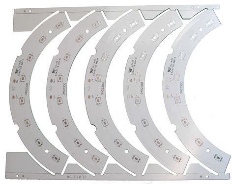
Introduction to IMS PCB
Insulated Metal Substrate (IMS) PCBs are a special type of printed circuit board that offer superior thermal management compared to traditional FR4 PCBs. IMS PCBs are designed to efficiently dissipate heat generated by electronic components, making them ideal for applications that require high power density or operate in harsh environments. In this article, we will explore the key features, manufacturing process, applications, and advantages of IMS PCBs.
What is an IMS PCB?
An IMS PCB consists of a metal substrate, typically aluminum, that is bonded to a thin layer of dielectric material, followed by a copper circuit layer. The metal substrate acts as a heat sink, quickly spreading and dissipating heat away from the electronic components. The dielectric layer provides electrical insulation between the metal substrate and the copper circuit layer, while also offering good thermal conductivity.
| Layer | Material | Function |
|---|---|---|
| Top Layer | Copper | Electrical circuit |
| Dielectric Layer | Thermal Interface Material (TIM) | Electrical insulation and thermal conductivity |
| Metal Substrate | Aluminum | Heat dissipation |
Key Features of IMS PCBs
- Excellent thermal conductivity
- High power density
- Improved reliability
- Reduced size and weight
- Enhanced mechanical stability
Manufacturing Process of IMS PCBs
Step 1: Substrate Preparation
The aluminum substrate is cleaned and treated to ensure good adhesion with the dielectric layer. The substrate thickness typically ranges from 0.5mm to 3mm, depending on the application requirements.
Step 2: Dielectric Layer Application
The dielectric layer, usually a thermal interface material (TIM), is applied to the aluminum substrate using various methods such as screen printing, roller coating, or lamination. The dielectric layer thickness is critical for ensuring good electrical insulation and thermal conductivity.
| Dielectric Material | Thermal Conductivity (W/mK) | Dielectric Strength (kV/mm) |
|---|---|---|
| Epoxy Resin | 1-2 | 20-50 |
| Polyimide | 0.2-0.5 | 100-200 |
| Ceramic Filled Polymer | 2-4 | 20-50 |
Step 3: Copper Foil Lamination
A thin layer of copper foil, typically 18µm to 105µm thick, is laminated onto the dielectric layer using heat and pressure. The copper foil acts as the conductive layer for the electrical circuit.
Step 4: Circuit Patterning
The desired circuit pattern is transferred onto the copper layer using photolithography and Etching Processes. This step is similar to the manufacturing of traditional FR4 PCBs.
Step 5: Surface Finishing
Various surface finishes, such as HASL, ENIG, or OSP, can be applied to the copper circuit layer to protect it from oxidation and improve solderability.
Step 6: Drilling and Cutting
Holes are drilled through the IMS PCB for component mounting and interconnections. The PCB is then cut to the desired shape and size using routing or punching techniques.

Applications of IMS PCBs
IMS PCBs are widely used in various industries and applications that require efficient heat dissipation and high power density. Some common applications include:
- Automotive electronics (e.g., LED headlights, engine control units)
- Power electronics (e.g., switch-mode power supplies, inverters)
- LED lighting (e.g., street lights, grow lights)
- Industrial controls (e.g., motor drives, sensors)
- Telecommunications (e.g., base stations, RF amplifiers)

Advantages of IMS PCBs
Superior Thermal Management
The metal substrate in IMS PCBs provides excellent thermal conductivity, allowing for efficient heat dissipation from electronic components. This helps to maintain lower operating temperatures, improving the reliability and lifespan of the components.
High Power Density
IMS PCBs can handle higher power densities compared to traditional FR4 PCBs, as they can dissipate heat more effectively. This allows for more compact designs and higher power applications.
Improved Reliability
By maintaining lower operating temperatures, IMS PCBs reduce thermal stress on electronic components, leading to improved reliability and longer product life.
Reduced Size and Weight
The efficient thermal management of IMS PCBs allows for more compact designs, as components can be placed closer together without the risk of overheating. This results in reduced size and weight of the overall electronic assembly.
Enhanced Mechanical Stability
The metal substrate in IMS PCBs provides excellent mechanical stability, making them more resistant to vibration and shock compared to traditional FR4 PCBs.

Challenges and Considerations
While IMS PCBs offer numerous advantages, there are some challenges and considerations to keep in mind:
- Higher material and manufacturing costs compared to FR4 PCBs
- Limited flexibility in design due to the metal substrate
- Potential for thermal expansion mismatch between layers
- Require specialized design and manufacturing expertise
Conclusion
IMS PCBs are a valuable solution for applications that demand efficient thermal management and high power density. By leveraging the advantages of a metal substrate and a thin dielectric layer, IMS PCBs can dissipate heat more effectively, leading to improved reliability, reduced size and weight, and enhanced mechanical stability. Despite the challenges and considerations involved, IMS PCBs have proven to be a superior choice for many industries and applications, driving innovation and performance in the world of electronics.
Frequently Asked Questions (FAQ)
1. What is the difference between IMS PCBs and traditional FR4 PCBs?
IMS PCBs feature a metal substrate, typically aluminum, that provides excellent thermal conductivity for heat dissipation. Traditional FR4 PCBs, on the other hand, are made of a glass-reinforced epoxy laminate that has lower thermal conductivity. IMS PCBs are designed for applications that require efficient heat dissipation and high power density, while FR4 PCBs are more suitable for general-purpose electronics.
2. Can IMS PCBs be used for flexible circuits?
No, IMS PCBs are not suitable for flexible circuits due to the rigid metal substrate. For applications that require flexibility, alternative materials such as polyimide or flexible Copper-Clad Laminates should be considered.
3. How does the thickness of the dielectric layer affect the performance of an IMS PCB?
The thickness of the dielectric layer is a critical factor in balancing electrical insulation and thermal conductivity. A thinner dielectric layer provides better thermal conductivity but may compromise electrical insulation. Conversely, a thicker dielectric layer offers better electrical insulation but may limit thermal conductivity. The optimal thickness depends on the specific application requirements and the properties of the chosen dielectric material.
4. Are IMS PCBs more expensive than traditional FR4 PCBs?
Yes, IMS PCBs are generally more expensive than traditional FR4 PCBs due to the higher material costs and specialized manufacturing processes involved. However, the improved thermal management and reliability offered by IMS PCBs can lead to cost savings in the long run, particularly for applications that operate in harsh environments or require high power density.
5. Can IMS PCBs be used in combination with other thermal management techniques?
Yes, IMS PCBs can be used in combination with other thermal management techniques, such as heatsinks, fans, or liquid cooling systems, to further enhance heat dissipation. The metal substrate of IMS PCBs provides an excellent interface for attaching additional thermal management components, allowing for even more effective cooling of electronic assemblies.

Leave a Reply