What is Chemical Etching?
Chemical etching, also known as wet etching, is a process that uses liquid chemicals to remove material from a substrate. The process involves immersing the substrate in an etchant solution that selectively dissolves the exposed areas while leaving the masked areas intact. The most common types of chemical etchants used in the semiconductor industry are:
- Hydrofluoric acid (HF) for etching silicon dioxide (SiO2)
- Potassium hydroxide (KOH) for etching silicon (Si)
- Phosphoric acid (H3PO4) for etching aluminum (Al)
- Nitric acid (HNO3) for etching copper (Cu)
The chemical etching process can be further classified into isotropic and anisotropic etching based on the etch profile.
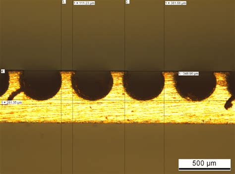
Isotropic Chemical Etching
Isotropic etching is a process where the etchant removes material at the same rate in all directions, resulting in a rounded or undercut etch profile. This type of etching is suitable for applications that require a more gentle and less precise material removal, such as removing sacrificial layers or creating through-holes.
Anisotropic Chemical Etching
Anisotropic etching, on the other hand, is a process where the etchant removes material at different rates depending on the crystallographic orientation of the substrate. This results in a more directional and controlled etch profile, with sidewalls that are either vertical or have a specific angle. Anisotropic chemical etching is commonly used for creating high-aspect-ratio structures, such as deep trenches or cavities, in single-crystal silicon substrates using KOH or tetramethylammonium hydroxide (TMAH) etchants.
What is Plasma Etching?
Plasma etching, also known as dry etching, is a process that uses a plasma (an ionized gas) to remove material from a substrate. The process involves generating a plasma in a vacuum chamber by applying a strong electromagnetic field to a gas, which ionizes the gas molecules and creates reactive species. These reactive species then interact with the exposed areas of the substrate, leading to material removal through physical sputtering, chemical reactions, or a combination of both.
Plasma etching can be categorized into three main types based on the dominant etching mechanism:
- Physical plasma etching (ion milling)
- Chemical plasma etching (plasma etching)
- Reactive ion etching (RIE)
Physical Plasma Etching (Ion Milling)
Physical plasma etching, or ion milling, is a process that relies on the physical sputtering of material by energetic ions. In this process, an inert gas, such as argon (Ar), is ionized to create a plasma. The ions are then accelerated towards the substrate by an electric field, where they collide with the surface and physically remove material through momentum transfer. Ion milling is highly anisotropic and can produce vertical sidewalls, but it has a low selectivity and can cause surface damage due to the high-energy ion bombardment.
Chemical Plasma Etching
Chemical plasma etching is a process that uses the chemical reactivity of the plasma species to remove material from the substrate. In this process, a reactive gas, such as sulfur hexafluoride (SF6) for etching silicon or oxygen (O2) for etching organic materials, is ionized to create a plasma. The reactive species in the plasma chemically react with the exposed areas of the substrate, forming volatile compounds that are pumped away by the vacuum system. Chemical plasma etching is highly selective and can have a high etch rate, but it is typically isotropic and can result in undercutting of the mask.
Reactive Ion Etching (RIE)
Reactive ion etching (RIE) is a process that combines the physical sputtering of ion milling with the chemical reactivity of plasma etching. In this process, a reactive gas is ionized to create a plasma, and the ions are accelerated towards the substrate by an electric field. The ions physically bombard the surface while also chemically reacting with the material, resulting in a synergistic etching effect. RIE can produce highly anisotropic etch profiles with good selectivity, making it a popular choice for etching patterns in semiconductor fabrication.

Differences between Chemical and Plasma Etching
Now that we have a basic understanding of chemical and plasma Etching Processes, let’s compare their key differences in terms of mechanism, capabilities, and applications.
| Aspect | Chemical Etching | Plasma Etching |
|---|---|---|
| Mechanism | Liquid-based chemical dissolution | Gas-based physical sputtering, chemical reactions, or a combination of both |
| Etch Profile | Isotropic (rounded) or anisotropic (crystallographic) | Anisotropic (vertical or tapered) |
| Selectivity | High selectivity between materials | Moderate to high selectivity, depending on the process |
| Etch Rate | Slow to moderate, depending on the etchant and material | Fast, especially for RIE processes |
| Substrate Damage | Minimal, as it is a gentle process | Potential for surface damage due to ion bombardment |
| Aspect Ratio | Limited by the isotropic nature of most etchants | High aspect ratios achievable, especially with RIE |
| Cost | Low cost, simple equipment setup | Higher cost, complex equipment setup |
| Environmental Impact | Wet chemicals require proper handling and disposal | Minimal waste, but toxic gases need to be handled safely |
Mechanism
The main difference between chemical and plasma etching lies in their etching mechanism. Chemical etching relies on the selective dissolution of material by liquid etchants, while plasma etching uses ionized gases to remove material through physical sputtering, chemical reactions, or a combination of both.
Etch Profile
Chemical etching can produce isotropic or anisotropic etch profiles, depending on the etchant and the substrate’s crystallographic orientation. Isotropic etching results in rounded or undercut profiles, while anisotropic etching can create sidewalls with specific angles. Plasma etching, on the other hand, is primarily anisotropic and can produce vertical or tapered sidewalls, depending on the process parameters.
Selectivity
Both chemical and plasma etching can have high selectivity between different materials, but the selectivity depends on the specific etchant or plasma chemistry used. Chemical etching can have extremely high selectivity, as the etchant can be chosen to selectively dissolve one material while leaving others intact. Plasma etching selectivity can be tuned by adjusting the gas composition, power, and pressure, but it may not reach the same level of selectivity as chemical etching.
Etch Rate
Plasma etching, especially RIE processes, generally has a higher etch rate compared to chemical etching. This is because plasma etching combines physical sputtering with chemical reactions, which can accelerate the material removal process. Chemical etching etch rates are typically slower and depend on the etchant concentration, temperature, and material being etched.
Substrate Damage
Chemical etching is generally considered a gentler process than plasma etching, as it does not involve high-energy ion bombardment. This means that chemical etching is less likely to cause surface damage or introduce defects in the substrate. Plasma etching, particularly physical plasma etching, can cause surface damage due to the energetic ions striking the substrate surface.
Aspect Ratio
Plasma etching, particularly RIE processes, can achieve higher aspect ratios compared to chemical etching. This is because plasma etching is inherently anisotropic and can create deep, narrow features with vertical sidewalls. Chemical etching is limited by the isotropic nature of most etchants, which can lead to undercutting and lower aspect ratios.
Cost
Chemical etching is generally less expensive than plasma etching, as it requires simpler equipment and can be performed in a wet bench setup. Plasma etching, on the other hand, requires sophisticated vacuum systems, power supplies, and gas handling equipment, which can significantly increase the cost of the process.
Environmental Impact
Both chemical and plasma etching processes have environmental considerations. Chemical etching uses wet chemicals that must be properly handled, stored, and disposed of to minimize environmental impact. Plasma etching uses gases that can be toxic or contribute to greenhouse gas emissions, but the process itself generates minimal liquid waste.

Applications of Chemical and Plasma Etching
Chemical and plasma etching find applications in various stages of semiconductor fabrication, as well as in other industries such as MEMS, microfluidics, and photonics.
Chemical Etching Applications
- Bulk micromachining of silicon using anisotropic etchants like KOH or TMAH
- Removing sacrificial layers in surface micromachining processes
- Etching metal layers, such as aluminum or copper, in interconnect fabrication
- Creating through-holes or vias in printed circuit boards (PCBs)
- Texturing surfaces to improve adhesion or optical properties
Plasma Etching Applications
- Etching high-aspect-ratio features, such as deep trenches or holes, in silicon using the Bosch process (alternating steps of SF6 etching and C4F8 passivation)
- Patterning gate electrodes and spacers in CMOS transistor fabrication
- Etching dielectric layers, such as silicon dioxide or silicon nitride, in MEMS and photonics devices
- Removing organic materials, such as photoresists or polymers, using oxygen plasma
- Etching compound semiconductors, such as gallium arsenide (GaAs) or indium phosphide (InP), for optoelectronic devices

Frequently Asked Questions (FAQ)
-
Q: Can chemical etching achieve the same level of anisotropy as plasma etching?
A: In general, chemical etching is more isotropic than plasma etching, as the etchant attacks the material equally in all directions. However, anisotropic chemical etching can be achieved using etchants that have different etch rates depending on the crystallographic orientation of the substrate, such as KOH or TMAH for single-crystal silicon. -
Q: What is the main advantage of plasma etching over chemical etching?
A: The main advantage of plasma etching is its ability to produce highly anisotropic etch profiles with vertical sidewalls, which is essential for creating high-aspect-ratio features in semiconductor devices. Plasma etching also typically has a higher etch rate than chemical etching, which can lead to faster processing times. -
Q: Are there any materials that cannot be etched using chemical or plasma etching?
A: Most materials used in semiconductor fabrication can be etched using either chemical or plasma etching, as long as the appropriate etchant or plasma chemistry is used. However, some materials, such as gold or platinum, are difficult to etch using conventional methods and may require specialized etching techniques, such as ion beam etching or electrochemical etching. -
Q: What safety precautions should be taken when performing chemical or plasma etching?
A: Both chemical and plasma etching processes involve hazardous materials and require proper safety precautions. When handling wet chemicals for chemical etching, appropriate personal protective equipment (PPE), such as gloves, goggles, and aprons, should be worn. Plasma etching processes use toxic and corrosive gases that must be properly contained and ventilated. All etching processes should be performed in a well-ventilated area with appropriate safety interlocks and emergency shut-off mechanisms. -
Q: Can chemical and plasma etching be used together in a single fabrication process?
A: Yes, chemical and plasma etching can be used together in a fabrication process, as they have complementary strengths and weaknesses. For example, a process may use chemical etching to remove a sacrificial layer and then use plasma etching to create high-aspect-ratio features in the underlying material. By combining both etching techniques, a wider range of structures and devices can be fabricated.
Conclusion
In conclusion, chemical and plasma etching are two essential processes in semiconductor manufacturing, each with its own unique mechanisms, capabilities, and applications. Chemical etching uses liquid etchants to selectively dissolve materials, while plasma etching uses ionized gases to remove material through physical sputtering, chemical reactions, or a combination of both. Chemical etching is generally more isotropic, has higher selectivity, and is less expensive, while plasma etching is more anisotropic, has higher etch rates, and can achieve higher aspect ratios.
Understanding the differences between these two etching processes is crucial for designing and fabricating semiconductor devices, as well as for optimizing process flows and troubleshooting manufacturing issues. By leveraging the strengths of both chemical and plasma etching, engineers can create complex structures and devices with the desired performance and reliability.
As the semiconductor industry continues to advance, new etching techniques and chemistries will be developed to meet the ever-increasing demands for smaller feature sizes, higher aspect ratios, and novel materials. However, the fundamental principles of chemical and plasma etching will remain essential tools in the fabrication of cutting-edge electronic and photonic devices.


Leave a Reply