What is PCB Etching?
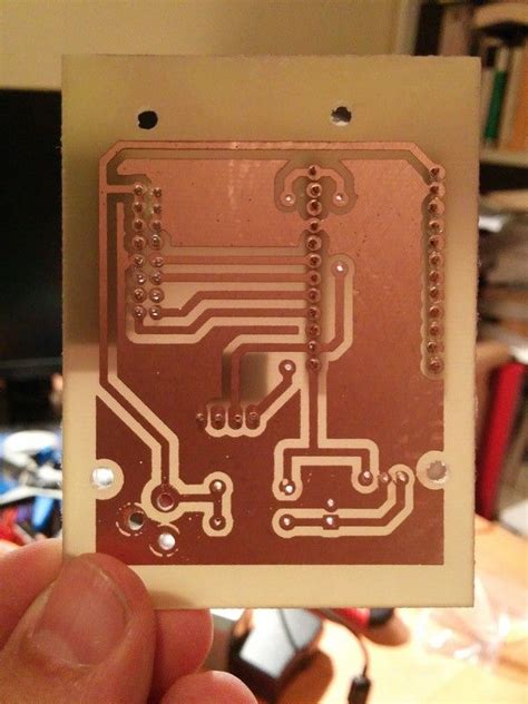
PCB etching is a critical step in the manufacturing process of printed circuit boards (PCBs). It involves selectively removing unwanted copper from the surface of the PCB substrate to create the desired conductive traces and pads that form the electrical connections of the circuit.
The etching process can be applied to both outer layers and inner layers of multi-layer PCBs. Etching the inner layers is especially important as it creates the interconnections between different layers of the board.
In this article, we will dive deep into the process of etching inner layers in PCB production, exploring the different methods, materials, and considerations involved. Whether you are an electronics engineer, PCB designer, or just curious about how PCBs are made, this comprehensive guide will provide you with valuable insights.
Types of PCB Etching Processes
There are two main types of PCB etching processes commonly used in the industry:
-
Wet Etching: This method involves immersing the PCB in a chemical etchant solution that selectively dissolves the exposed copper while leaving the protected areas intact. The most common etchant used for wet etching is ferric chloride (FeCl3).
-
Dry Etching: Also known as plasma etching, this method uses a plasma (ionized gas) to remove the unwanted copper. The PCB is placed in a vacuum chamber where a reactive gas is introduced and ionized using a high-frequency electric field. The plasma reacts with the exposed copper, converting it into volatile compounds that are then removed from the chamber.
While wet etching is the more traditional and widely used method, dry etching has gained popularity in recent years due to its higher precision, better environmental friendliness, and ability to etch finer features.

The Inner Layer Etching Process
Step 1: Inner Layer Material Selection
The first step in etching inner layers is selecting the appropriate PCB substrate material. The most common materials used for inner layers are:
- FR-4: A glass-reinforced epoxy laminate that offers good mechanical and electrical properties.
- Polyimide: A high-performance polymer that provides excellent thermal stability and flexibility.
- PTFE (Teflon): A low-dielectric material that is suitable for high-frequency applications.
The choice of material depends on the specific requirements of the PCB, such as the operating environment, electrical performance, and cost considerations.
Step 2: Inner Layer Patterning
Once the substrate material is selected, the desired circuit pattern needs to be transferred onto the inner layer. This is typically done using a photolithography process:
- The inner layer is coated with a light-sensitive photoresist material.
- The photoresist is exposed to UV light through a photomask that contains the circuit pattern.
- The exposed areas of the photoresist are developed, revealing the underlying copper.
- The unexposed areas of the photoresist are removed, leaving a protective layer over the copper that will form the final Circuit Traces.
Step 3: Etching the Inner Layer
With the circuit pattern defined, the inner layer is ready for etching. The specific etching process depends on whether wet or dry etching is used.
Wet Etching Process
- The patterned inner layer is immersed in a tank containing the etchant solution (usually ferric chloride).
- The etchant chemically reacts with the exposed copper, dissolving it and leaving behind the protected copper traces.
- The etching process is carefully monitored and controlled to ensure uniform removal of the copper.
- Once etching is complete, the inner layer is rinsed with water to remove any residual etchant.
Dry Etching Process
- The patterned inner layer is placed in a vacuum chamber.
- A reactive gas (such as chlorine or fluorine) is introduced into the chamber and ionized using a high-frequency electric field, forming a plasma.
- The plasma reacts with the exposed copper, converting it into volatile compounds that are removed from the chamber by the vacuum system.
- The etching process is precisely controlled by adjusting parameters such as gas flow rate, pressure, and temperature.
Step 4: Stripping and Cleaning
After etching, the remaining photoresist needs to be stripped from the inner layer. This is typically done using a chemical stripper that dissolves the photoresist without damaging the copper traces.
The inner layer is then thoroughly cleaned to remove any residues or contaminants that may have been introduced during the etching process. Common cleaning methods include:
- Ultrasonic cleaning: The inner layer is placed in an ultrasonic bath containing a cleaning solution and subjected to high-frequency sound waves that agitate the solution and dislodge contaminants.
- Plasma cleaning: The inner layer is exposed to a low-pressure plasma that reacts with and removes organic contaminants from the surface.
Step 5: Inspection and Quality Control
Before proceeding to the next stages of PCB Fabrication, the etched inner layer undergoes a rigorous inspection and quality control process to ensure that it meets the required specifications. Some common inspection techniques include:
- Automated Optical Inspection (AOI): The inner layer is scanned using a high-resolution camera and image processing algorithms to detect any defects or deviations from the intended design.
- Electrical Testing: The inner layer is subjected to various electrical tests, such as continuity and isolation tests, to verify the integrity of the copper traces and the absence of short circuits or open connections.
Any defective inner layers are identified and removed from the production line at this stage to prevent them from being incorporated into the final PCB Assembly.

Advantages and Disadvantages of Different Etching Methods
| Etching Method | Advantages | Disadvantages |
|---|---|---|
| Wet Etching | – Lower cost – Simpler equipment – Suitable for larger features |
– Lower precision – Isotropic etching (undercut) – Environmental concerns (hazardous chemicals) |
| Dry Etching | – Higher precision – Anisotropic etching (vertical sidewalls) – Environmentally friendly |
– Higher cost – More complex equipment – Slower etch rates |

Challenges and Considerations in Inner Layer Etching
Etching inner layers presents several challenges and considerations that need to be addressed to ensure the quality and reliability of the final PCB:
-
Etch Factor: The etch factor is the ratio of the etch depth to the undercut (lateral etching). A high etch factor is desirable to achieve well-defined traces with minimal undercut. The etch factor can be influenced by factors such as the etchant concentration, temperature, and agitation.
-
Etchant Control: Maintaining the correct composition and concentration of the etchant solution is crucial for consistent etching results. The etchant needs to be regularly monitored and replenished to compensate for the depletion of active ingredients during the etching process.
-
Undercutting: Undercutting refers to the lateral etching of the copper beneath the photoresist layer, resulting in traces that are narrower than intended. Minimizing undercutting is important to maintain the integrity and performance of the circuit. This can be achieved by optimizing the etching parameters and using high-resolution photoresists.
-
Etch Rate Uniformity: Ensuring a uniform etch rate across the entire inner layer is essential to avoid over-etching or under-etching in certain areas. Factors such as the etchant flow pattern, agitation, and temperature distribution need to be carefully controlled to achieve uniform etching.
-
Registration and Alignment: In multi-layer PCBs, the inner layers need to be precisely aligned with each other and with the outer layers to ensure proper interconnections. Any misalignment during the etching process can lead to poor electrical connections or even short circuits. High-precision alignment systems and registration marks are used to maintain the required accuracy.
-
Handling and Contamination: Inner layers are delicate and susceptible to damage or contamination during handling. Proper handling procedures, such as using gloves and clean room environments, are essential to prevent any foreign particles or oils from contaminating the surfaces and affecting the etching process.
Frequently Asked Questions (FAQ)
1. What is the difference between inner layer and outer layer etching?
Inner layer etching refers to the process of etching the conductive patterns on the internal layers of a multi-layer PCB, while outer layer etching deals with the top and bottom layers of the PCB. The main difference lies in the accessibility of the layers. Inner layers are sandwiched between other layers and require additional steps, such as lamination and drilling, to create interconnections. Outer layers, being exposed, can be directly etched and processed.
2. Can both wet and dry etching be used for inner layers?
Yes, both wet and dry etching methods can be used for etching inner layers. The choice depends on factors such as the desired feature size, etch precision, environmental considerations, and production volume. Wet etching is more commonly used due to its simplicity and lower cost, while dry etching is preferred for high-precision and fine-pitch applications.
3. What is the role of the photoresist in inner layer etching?
The photoresist is a light-sensitive polymer that is used to transfer the desired circuit pattern onto the inner layer. It acts as a protective mask, shielding the areas of the copper that will form the final circuit traces from the etchant. The photoresist is selectively exposed to UV light through a photomask, developed, and then used to selectively remove the unwanted copper during the etching process.
4. How does the choice of substrate material affect inner layer etching?
The choice of substrate material can affect the etching process in several ways. Different materials have different chemical and physical properties that influence their interaction with the etchant. For example, some materials may etch faster or slower than others, requiring adjustments to the etching parameters. Additionally, the surface roughness and adhesion properties of the substrate can impact the uniformity and quality of the etched features.
5. What are some common defects that can occur during inner layer etching?
Some common defects that can occur during inner layer etching include:
- Overetching: Excessive removal of copper, resulting in traces that are narrower than intended or even complete loss of features.
- Underetching: Insufficient removal of copper, leading to traces that are wider than intended or short circuits between adjacent features.
- Undercutting: Lateral etching beneath the photoresist layer, causing traces to have sloped or undercut sidewalls.
- Etchant residues: Incomplete removal of etchant or byproducts, leaving behind contaminants that can affect the performance or reliability of the PCB.
- Misalignment: Inaccurate registration or alignment of the inner layer with respect to other layers or features.
Careful process control, regular maintenance, and thorough inspection can help minimize the occurrence of these defects and ensure the quality of the etched inner layers.
Conclusion
Etching inner layers is a critical step in the production of multi-layer PCBs, enabling the creation of complex interconnections and circuitry. The process involves selectively removing unwanted copper from the surface of the inner layer substrate using either wet or dry etching methods.
Wet etching, using chemical etchants like ferric chloride, is the more traditional and widely used approach, offering simplicity and cost-effectiveness. Dry etching, using plasma technology, provides higher precision and environmental benefits but comes with increased complexity and cost.
Regardless of the chosen method, careful control of the etching parameters, proper handling and contamination prevention, and thorough inspection and quality control are essential to ensure the quality and reliability of the etched inner layers.
As PCB designs continue to evolve with increasing complexity and miniaturization, advancements in inner layer etching technologies will play a crucial role in enabling the fabrication of high-performance and reliable multi-layer PCBs.
By understanding the intricacies of inner layer etching, electronics engineers, PCB designers, and manufacturers can make informed decisions and optimize their processes to achieve the desired results in PCB production.


Leave a Reply