Introduction to PCB Development
Printed Circuit Boards (PCBs) have revolutionized the electronics industry since their inception in the early 20th century. PCBs are the backbone of modern electronic devices, providing a reliable and efficient means of connecting electronic components. The development of PCBs has been a continuous process, driven by advancements in technology and the increasing demand for smaller, faster, and more complex electronic devices.
Early History of PCBs
The concept of PCBs can be traced back to the early 1900s when Albert Hanson, a German inventor, filed a patent for a “printed wire” that could be used to connect electronic components. However, it wasn’t until the 1920s that the first PCBs were actually produced. These early PCBs were made using a process called “through-hole” technology, where holes were drilled into a board and components were inserted and soldered in place.
The Rise of Through-Hole Technology
Through-hole technology remained the standard for PCB production for several decades. In the 1950s, the U.S. military began using PCBs in their electronic equipment, which helped to drive the development of new PCB manufacturing techniques. By the 1960s, PCBs were being used in a wide range of electronic devices, from radios and televisions to computers and aerospace equipment.
Advancements in PCB Technology
Surface Mount Technology (SMT)
In the 1980s, a new PCB manufacturing technique called Surface Mount Technology (SMT) was introduced. SMT allowed for smaller components to be mounted directly onto the surface of the PCB, eliminating the need for through-hole mounting. This allowed for smaller, more compact PCBs to be produced, which was essential for the development of portable electronic devices like mobile phones and laptops.
Multi-Layer PCBs
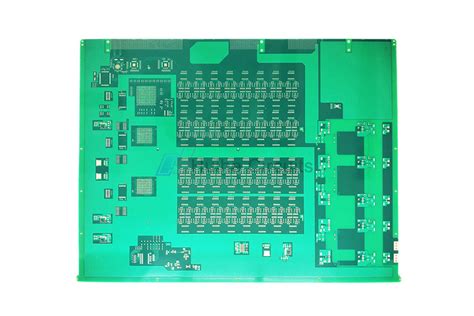
As electronic devices became more complex, the need for more sophisticated PCBs grew. In the 1990s, multi-layer PCBs were developed, which allowed for even greater component density and more complex circuit designs. Multi-layer PCBs are made by stacking multiple layers of PCB material and connecting them with vias, which are small holes that allow signals to pass between layers.
Benefits of Multi-Layer PCBs
Multi-layer PCBs offer several benefits over single-layer PCBs, including:
- Increased component density
- Improved signal integrity
- Better power distribution
- Reduced electromagnetic interference (EMI)
| Layer Count | Typical Application |
|---|---|
| 1-2 | Simple circuits |
| 4 | Digital circuits |
| 6 | Complex digital circuits |
| 8+ | High-speed digital, RF, and mixed-signal circuits |
High-Density Interconnect (HDI) PCBs
In the early 2000s, High-Density Interconnect (HDI) PCBs were developed to meet the demands of increasingly complex electronic devices. HDI PCBs use advanced manufacturing techniques like microvias and buried/blind vias to achieve even greater component density and signal integrity.
HDI PCB Manufacturing Techniques
| Technique | Description |
|---|---|
| Microvias | Small vias (<150 μm) that connect adjacent layers |
| Buried/Blind Vias | Vias that do not extend through the entire board thickness |
| Sequential Lamination | Building up layers one at a time to create complex stack-ups |
| Via-in-Pad | Placing vias directly in component pads for higher density |
PCB Design and Simulation
Electronic Design Automation (EDA) Tools
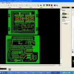
As PCBs have become more complex, the need for sophisticated design and simulation tools has grown. Electronic Design Automation (EDA) tools allow PCB designers to create, simulate, and optimize their designs before sending them to manufacturing. Some popular EDA tools include:
- Altium Designer
- Cadence Allegro
- Mentor Graphics PADS
- KiCad (open source)
PCB Design Considerations
When designing a PCB, there are several key considerations that must be taken into account, including:
- Component selection and placement
- Signal integrity and power distribution
- Thermal management
- Manufacturing constraints (e.g., minimum trace width, via size)
- Electromagnetic compatibility (EMC)
PCB Simulation Techniques
PCB simulation allows designers to test and optimize their designs before manufacturing. Some common PCB simulation techniques include:
- Signal integrity analysis
- Power integrity analysis
- Electromagnetic interference (EMI) analysis
- Thermal analysis

PCB Manufacturing Process
PCB Fabrication
Once a PCB design is complete, it is sent to a fabrication house for manufacturing. The PCB fabrication process typically involves the following steps:
- Material selection and preparation
- Copper etching and plating
- Lamination and drilling
- Solder mask and silkscreen application
- Surface finish application (e.g., HASL, ENIG, OSP)
PCB Assembly
After fabrication, the PCB is sent to an assembly house where components are attached using techniques like SMT or through-hole soldering. The PCB assembly process typically involves the following steps:
- Solder paste application (for SMT)
- Component placement
- Soldering (reflow for SMT, wave for through-hole)
- Inspection and testing
Quality Control and Testing
Quality control and testing are critical steps in the PCB manufacturing process. Some common quality control and testing techniques include:
- Visual inspection
- Automated optical inspection (AOI)
- X-ray inspection
- In-circuit testing (ICT)
- Functional testing
Future of PCB Development
Emerging Technologies
As electronic devices continue to evolve, so too will PCBs. Some emerging technologies that are likely to shape the future of PCB development include:
- Flexible and stretchable PCBs
- 3D printing of PCBs
- Embedded components
- Optical interconnects
Challenges and Opportunities
The future of PCB development presents both challenges and opportunities. Some key challenges include:
- Miniaturization and increased component density
- Signal integrity and power distribution at high frequencies
- Thermal management in high-power applications
- Environmental concerns (e.g., lead-free soldering, recycling)
Despite these challenges, there are also many opportunities for innovation and growth in the PCB industry. As new technologies emerge and demand for advanced electronic devices continues to grow, PCB designers and manufacturers will need to adapt and innovate to stay competitive.
Frequently Asked Questions (FAQ)
- What is a PCB?
-
A PCB, or Printed Circuit Board, is a board made of insulating material with conductive tracks and pads etched onto its surface. It is used to mechanically support and electrically connect electronic components using conductive pathways.
-
What are the different types of PCBs?
-
There are several types of PCBs, including:
- Single-layer PCBs: have conductive tracks on one side only
- Double-layer PCBs: have conductive tracks on both sides
- Multi-layer PCBs: have conductive tracks on multiple layers separated by insulating material
- Flexible PCBs: use flexible substrate material for applications where flexibility is required
- Rigid-Flex PCBs: combine rigid and flexible sections for complex 3D designs
-
What is the difference between through-hole and surface mount technology?
-
Through-hole technology involves inserting component leads through holes drilled in the PCB and soldering them in place on the opposite side. Surface mount technology involves placing components directly onto pads on the surface of the PCB and soldering them in place without the need for holes.
-
What are some common PCB design software tools?
-
Some common PCB design software tools include:
- Altium Designer
- Cadence Allegro
- Mentor Graphics PADS
- KiCad (open source)
- Eagle (Autodesk)
-
What are some important considerations when designing a PCB?
- Some important considerations when designing a PCB include:
- Component selection and placement for optimal performance and manufacturing
- Signal integrity and power distribution to ensure reliable operation
- Thermal management to prevent overheating and ensure reliability
- Manufacturing constraints such as minimum trace width and spacing
- Electromagnetic compatibility (EMC) to prevent interference with other devices
Conclusion
PCBs have come a long way since their inception in the early 20th century. From simple single-layer boards to complex multi-layer HDI designs, PCBs have evolved to meet the ever-increasing demands of the electronics industry. As new technologies emerge and electronic devices become more advanced, PCB designers and manufacturers will need to continue to innovate and adapt to stay competitive. The future of PCB development is sure to bring both challenges and opportunities, but one thing is certain: PCBs will continue to play a critical role in shaping the electronic devices of tomorrow.
Leave a Reply