The Importance of Accurate PCB Drilling
Accurate PCB drilling is essential for several reasons:
-
Component Placement: Precise drilling ensures that components can be properly inserted and soldered onto the PCB. Misaligned or incorrectly sized holes can lead to difficulties during assembly and may even result in damaged components.
-
Electrical Connectivity: Drilled holes often serve as vias, which are used to connect different layers of a multi-layer PCB. Inaccurate drilling can cause issues with electrical connectivity, leading to signal integrity problems or even complete circuit failure.
-
Mechanical Stability: Mounting holes are drilled to allow the PCB to be securely attached to an enclosure or other mechanical components. Poor drilling can compromise the mechanical stability of the PCB, resulting in vibration, warping, or other physical damage.
PCB Drilling Techniques
There are two primary techniques used for PCB drilling:
Mechanical Drilling
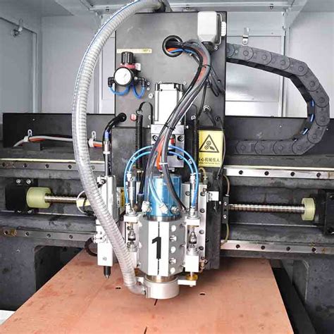
Mechanical drilling is the most common method for creating holes in PCBs. It involves using high-speed drill bits to physically remove material from the substrate. The process is typically performed using CNC (Computer Numerical Control) machines, which offer high precision and repeatability.
Advantages of mechanical drilling include:
– Versatility in hole sizes and shapes
– Suitable for a wide range of PCB materials
– Cost-effective for small to medium-sized production runs
Challenges of mechanical drilling include:
– Drill bit wear and breakage
– Potential for smear and burr formation
– Slower than laser drilling for high-volume production
Laser Drilling
Laser drilling is a more advanced technique that uses focused laser beams to vaporize the PCB material, creating holes without physical contact. This method is particularly useful for creating small, high-density holes and is often used in HDI (High-Density Interconnect) PCB designs.
Advantages of laser drilling include:
– Ability to create extremely small holes (down to 50 microns)
– High speed and throughput
– Minimal mechanical stress on the PCB
– Reduced risk of contamination
Challenges of laser drilling include:
– Higher equipment costs compared to mechanical drilling
– Limited material compatibility (some materials may not be suitable for laser drilling)
– Potential for thermal damage to the PCB substrate

Drilling Considerations in PCB Design
When designing a PCB, several factors related to drilling must be considered to ensure optimal results:
Hole Size and Tolerance
The size of the drilled holes should be carefully specified based on the requirements of the components and vias. It is important to consider the tolerance of the drilling process and ensure that the hole sizes are within acceptable limits. Designers should also take into account the potential for hole wall pullback and adjust the design accordingly.
| Hole Type | Typical Size Range |
|---|---|
| Component Holes | 0.5 mm – 2.5 mm |
| Via Holes | 0.2 mm – 0.8 mm |
| Mounting Holes | 2.0 mm – 6.0 mm |
Drill Bit Selection
The choice of drill bit is crucial for achieving accurate and clean holes. Factors to consider when selecting a drill bit include:
- Material compatibility
- Hole size and aspect ratio
- Flute design and coating
- Spindle speed and feed rate
Proper drill bit selection helps minimize issues such as drill wander, breakage, and excessive wear.
Drill Hit Positioning
The positioning of drill hits on the PCB layout should be optimized to minimize drill time and ensure consistent results. Designers should consider the following:
- Grouping similar hole sizes together
- Optimizing drill path to reduce travel distance
- Avoiding drilling too close to the edge of the PCB
- Providing adequate spacing between holes to maintain structural integrity
Layer Stack-Up and Drilling Sequence
In multi-layer PCBs, the layer stack-up and drilling sequence can impact the quality of the drilled holes. Designers should consider the following:
- Symmetrical layer stack-up to minimize warping and other physical distortions
- Drilling sequence that minimizes the risk of delamination and other layer-related issues
- Use of backing materials to reduce burr formation and improve hole quality

Best Practices for PCB Drilling
To achieve optimal results in PCB drilling, designers and manufacturers should adhere to the following best practices:
-
Use a comprehensive Drill File: Provide a detailed drill file that includes all necessary information, such as hole sizes, locations, and tolerances. This helps ensure accurate and efficient drilling.
-
Optimize Drill Hit Positioning: Carefully plan the positioning of drill hits to minimize drill time, reduce wear on drill bits, and ensure consistent results.
-
Select Appropriate Drill Bits: Choose drill bits that are compatible with the PCB material, hole size, and aspect ratio. Consider factors such as flute design, coating, and spindle speed.
-
Implement Proper Maintenance: Regular maintenance of drilling equipment, including cleaning, lubrication, and replacement of worn parts, helps ensure consistent performance and minimize downtime.
-
Monitor and Inspect: Implement robust quality control measures, including regular monitoring and inspection of drilled holes. Use statistical process control (SPC) techniques to identify and address any issues early in the manufacturing process.

FAQ
- What is the smallest hole size that can be achieved with mechanical drilling?
-
Mechanical drilling can typically achieve hole sizes down to 0.2 mm (0.008 inches) in diameter. However, the achievable hole size depends on factors such as the PCB material, thickness, and aspect ratio.
-
Can laser drilling be used for all PCB materials?
-
No, laser drilling is not suitable for all PCB materials. Some materials, such as certain ceramics and metal-backed substrates, may not be compatible with laser drilling due to their thermal properties or reflectivity.
-
How does drill bit wear affect the quality of drilled holes?
-
Drill bit wear can cause a range of issues, including enlarged or misshapen holes, rough hole walls, and burr formation. As drill bits wear, they lose their sharpness and can generate more heat, leading to reduced hole quality and potential damage to the PCB.
-
What is the purpose of vias in PCB design?
-
Vias are used to create electrical connections between different layers of a multi-layer PCB. They allow signals and power to be routed vertically through the board, enabling more complex and compact circuit designs.
-
How can designers minimize the risk of delamination during drilling?
- To minimize the risk of delamination, designers should consider using a symmetrical layer stack-up, selecting appropriate drill bits and drilling parameters, and optimizing the drilling sequence. The use of backing materials and proper control of drilling temperature can also help reduce the risk of delamination.
Conclusion
Drilling is a critical process in PCB design and manufacturing, directly impacting the functionality, reliability, and quality of the final product. By understanding the importance of accurate drilling, the available techniques, and the key considerations in PCB design, designers and manufacturers can optimize the drilling process and achieve superior results.
Effective PCB drilling requires a combination of careful design, appropriate equipment selection, and adherence to best practices. By providing comprehensive drill files, optimizing drill hit positioning, selecting suitable drill bits, implementing proper maintenance, and monitoring the process closely, designers and manufacturers can ensure consistently high-quality drilled holes.
As PCB technologies continue to evolve, with increasing complexity and miniaturization, the importance of accurate and precise drilling will only continue to grow. By staying informed about the latest techniques, best practices, and industry standards, PCB designers and manufacturers can stay ahead of the curve and deliver cutting-edge products that meet the demands of today’s electronic devices.


Leave a Reply