What is PCB Panelization?
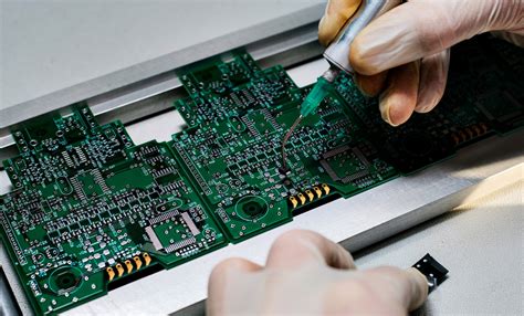
PCB panelization is the process of arranging multiple individual PCB Designs onto a single, larger panel. The panel is then fabricated as a single unit, allowing for the simultaneous production of multiple PCBs. After the manufacturing process, the individual boards are separated from the panel through a process called depaneling.
Benefits of PCB Panelization
-
Cost Reduction: By producing multiple PCBs on a single panel, the overall manufacturing costs are reduced. This is because the setup time and material costs are spread across a larger number of boards.
-
Increased Efficiency: Panelization allows for the simultaneous fabrication of multiple PCBs, which significantly reduces the production time compared to manufacturing each board individually.
-
Improved Yield: With panelization, the number of handling steps is minimized, reducing the risk of damage to individual boards. This leads to a higher yield and fewer defective boards.
-
Consistent Quality: Since all the boards on a panel are produced under the same conditions, panelization ensures consistent quality across the entire batch of PCBs.
PCB Panelization Methods
There are several methods used for PCB panelization, each with its own advantages and considerations. Let’s explore the most common techniques:
1. Tab Routing
Tab routing is a popular panelization method that involves connecting individual PCBs with small tabs. These tabs are designed to be easily breakable, allowing for the separation of boards after manufacturing. The tabs are typically located along the edges of the boards and can be perforated or scored to facilitate the depaneling process.
Advantages:
– Simple and cost-effective method
– Suitable for low-volume production
– Easy to implement
Considerations:
– Manual depaneling can be time-consuming
– Risk of damage to the boards during depaneling
– Limited control over the tab size and placement
2. V-Scoring
V-scoring is a panelization technique that involves creating V-shaped grooves between the individual PCBs on the panel. These grooves are cut partially through the panel, leaving a thin layer of material that holds the boards together. During depaneling, the boards can be easily separated by applying pressure along the V-scored lines.
Advantages:
– Precise and controlled depaneling process
– Minimal stress on the boards during separation
– Suitable for high-volume production
Considerations:
– Requires specialized equipment for V-scoring
– Limited flexibility in board placement and orientation
– Potential for visible score marks on the board edges
3. Mouse Bites
Mouse bites, also known as break-away tabs or perforations, are small, rounded notches placed along the edges of individual PCBs on the panel. These notches create weak points that allow for easy separation of the boards during depaneling. The size and spacing of the mouse bites can be adjusted based on the specific requirements of the project.
Advantages:
– Easy to design and implement
– Suitable for various board shapes and sizes
– Allows for manual or automated depaneling
Considerations:
– Visible mouse bite marks on the board edges
– Potential for rough edges after depaneling
– Reduced structural integrity of the panel
PCB Panelization Design Considerations
When designing a PCB panel, several key factors must be taken into account to ensure optimal results. Let’s discuss some of the essential design considerations:
1. Board Spacing and Clearance
Adequate spacing between individual PCBs on the panel is crucial to prevent interference and ensure proper depaneling. The spacing should account for the panelization method used, as well as any manufacturing tolerances. Additionally, sufficient clearance should be provided around the edges of the panel to allow for handling and processing.
2. Fiducial Markers
Fiducial markers are reference points placed on the panel that assist in aligning and orienting the boards during the manufacturing process. These markers are typically small, circular pads or crosshairs that are easily recognizable by automated assembly equipment. Proper placement and sizing of fiducial markers are essential for accurate board registration and consistent results.
3. Tooling Holes
Tooling holes are precisely positioned holes on the panel that are used to secure the panel during the fabrication and assembly processes. These holes ensure accurate alignment and prevent the panel from shifting or moving. The size, quantity, and location of tooling holes should be determined based on the specific requirements of the manufacturing equipment and the panel dimensions.
4. Panelization Border
A panelization border is an additional area around the perimeter of the panel that provides space for tooling holes, fiducial markers, and other panel-level features. The border should be designed to meet the minimum requirements of the fabrication and assembly processes while minimizing material waste. It is important to consider the panel size limitations and optimize the border dimensions accordingly.
5. Depaneling Method
The choice of depaneling method should be considered during the PCB panelization design phase. Different methods, such as tab routing, V-scoring, or mouse bites, have specific design requirements that must be incorporated into the panel layout. For example, tab routing requires the placement of tabs along the board edges, while V-scoring necessitates the inclusion of V-shaped grooves between the boards.

Best Practices for PCB Panelization
To ensure successful PCB panelization and optimize the manufacturing process, consider the following best practices:
-
Collaborate with the Manufacturer: Engage with your PCB manufacturer early in the design process to discuss panelization requirements, limitations, and recommendations. Their expertise can help you make informed decisions and avoid potential issues.
-
Optimize Panel Utilization: Maximize the number of PCBs per panel while maintaining proper spacing and clearance. Efficient panel utilization helps reduce material waste and lower production costs.
-
Consider Assembly Requirements: Take into account the assembly process when designing the panel. Ensure that the panelization method and layout are compatible with the assembly equipment and techniques used.
-
Test and Validate: Before mass production, conduct thorough testing and validation of the panelized design. This includes verifying the accuracy of the panel dimensions, ensuring proper board registration, and assessing the ease of depaneling.
-
Document and Communicate: Clearly document the panelization specifications, including panel dimensions, board spacing, tooling hole locations, and any special requirements. Communicate this information to all stakeholders involved in the manufacturing process to ensure consistency and avoid misunderstandings.
Frequently Asked Questions (FAQ)
-
Q: What is the minimum spacing required between PCBs on a panel?
A: The minimum spacing between PCBs on a panel depends on various factors, such as the panelization method, manufacturing capabilities, and board dimensions. Typically, a minimum spacing of 2-3 mm is recommended, but it is best to consult with your PCB manufacturer for specific guidelines. -
Q: Can different PCB designs be panelized together?
A: Yes, different PCB designs can be panelized together on the same panel, provided they have similar specifications and manufacturing requirements. This approach, known as mixed-panel assembly, can help optimize panel utilization and reduce production costs. -
Q: How do I choose the appropriate panelization method for my project?
A: The choice of panelization method depends on several factors, including the PCB design complexity, production volume, depaneling requirements, and manufacturing capabilities. Consult with your PCB manufacturer to determine the most suitable method based on your specific project needs. -
Q: Can PCB panelization be used for flexible circuits?
A: Yes, PCB panelization techniques can be applied to flexible circuits as well. However, the panelization design and methods may differ from those used for rigid PCBs. Special considerations, such as material properties and flexibility requirements, must be taken into account when panelizing flexible circuits. -
Q: How does PCB panelization affect the overall cost of production?
A: PCB panelization can significantly reduce the overall cost of production by optimizing the manufacturing process. By producing multiple PCBs on a single panel, setup times and material costs are minimized. However, the cost savings may vary depending on factors such as panel utilization, panelization method, and production volume.
Conclusion
PCB panelization is a crucial technique in the electronics manufacturing industry that offers numerous benefits, including cost reduction, increased efficiency, improved yield, and consistent quality. By understanding the different panelization methods, design considerations, and best practices, engineers and manufacturers can optimize their PCB production processes.
When implementing PCB panelization, it is essential to collaborate with experienced PCB Manufacturers, carefully consider the specific requirements of the project, and conduct thorough testing and validation. By following the guidelines and best practices outlined in this article, you can ensure successful PCB panelization and achieve optimal results in your electronics manufacturing endeavors.
Leave a Reply