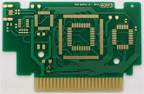
Introduction to Copper PCB
Printed Circuit Boards (PCBs) are the backbone of modern electronics, providing a reliable and efficient means of connecting electronic components. One of the most critical materials used in the manufacturing of PCBs is copper foil. Copper is an excellent conductor of electricity and heat, making it the ideal choice for creating conductive pathways on PCBs. In this article, we will explore the role of copper foil in PCBs, its properties, manufacturing processes, and applications.
What is Copper Foil?
Copper foil is a thin sheet of copper that is used in the production of PCBs. It is typically made by electrodeposition, where a thin layer of copper is deposited onto a rotating drum or continuous belt. The thickness of the copper foil can vary depending on the application, but it typically ranges from 18 to 70 microns (μm).
Properties of Copper Foil
Copper foil has several properties that make it an ideal material for use in PCBs:
- High electrical conductivity
- Excellent thermal conductivity
- Good mechanical strength
- Resistance to corrosion
- Ease of soldering
These properties enable copper foil to efficiently conduct electrical signals, dissipate heat, and maintain the structural integrity of the PCB.
Manufacturing Process of Copper PCB
PCB Substrate Preparation
The first step in manufacturing a copper PCB is to prepare the substrate. The substrate is typically made of a non-conductive material, such as FR-4 (a glass-reinforced epoxy laminate). The substrate is cleaned and treated to ensure proper adhesion of the copper foil.
Copper Foil Lamination
Once the substrate is prepared, the copper foil is laminated onto it using heat and pressure. The lamination process ensures a strong bond between the copper foil and the substrate, preventing delamination during the subsequent manufacturing steps.
Photoresist Application
A photoresist layer is then applied to the copper foil. The photoresist is a light-sensitive material that hardens when exposed to ultraviolet (UV) light. The photoresist layer is used to transfer the desired circuit pattern onto the copper foil.
Exposure and Development
The PCB is then exposed to UV light through a photomask, which contains the circuit pattern. The areas of the photoresist that are exposed to UV light become soluble in a developing solution, while the unexposed areas remain insoluble. The PCB is then developed, removing the soluble photoresist and revealing the desired circuit pattern on the copper foil.
Etching
The exposed copper foil is then etched away using a chemical solution, typically ferric chloride or ammonium persulfate. The etching process removes the unwanted copper, leaving only the desired circuit pattern on the substrate.
Finishing
Finally, the PCB undergoes various finishing processes, such as solder mask application, silkscreen printing, and surface finishing (e.g., HASL, ENIG, or OSP). These processes protect the copper traces, improve solderability, and provide a professional appearance to the finished PCB.

Types of Copper Foil
There are two main types of copper foil used in PCB manufacturing:
- Electrodeposited (ED) Copper Foil
- Rolled Annealed (RA) Copper Foil
Electrodeposited (ED) Copper Foil
ED copper foil is produced by electrodeposition, where copper ions are deposited onto a rotating drum or continuous belt. ED copper foil has a fine-grained structure and a matte side and a shiny side. The matte side is typically used for lamination to the PCB substrate, as it provides better adhesion due to its rough surface.
ED copper foil is available in various thicknesses, typically ranging from 18 to 70 μm. The most common thicknesses used in PCB manufacturing are:
| Thickness (μm) | Weight (oz/ft²) |
|---|---|
| 18 | 0.5 |
| 35 | 1.0 |
| 70 | 2.0 |
Rolled Annealed (RA) Copper Foil
RA copper foil is produced by rolling and annealing high-purity copper ingots. The rolling process reduces the thickness of the copper, while annealing helps to improve its ductility and flexibility. RA copper foil has a more uniform grain structure compared to ED copper foil, resulting in better mechanical properties and improved resistance to fatigue.
RA copper foil is available in thicknesses ranging from 35 to 350 μm. However, due to its higher cost and limited availability, RA copper foil is less commonly used in PCB manufacturing compared to ED copper foil.

Applications of Copper PCB
Copper PCBs are used in a wide range of applications, including:
- Consumer electronics (smartphones, laptops, televisions, etc.)
- Automotive electronics (engine control units, infotainment systems, sensors, etc.)
- Industrial equipment (automation systems, power supplies, motor controllers, etc.)
- Medical devices (patient monitors, imaging systems, diagnostic equipment, etc.)
- Aerospace and defense systems (avionics, radar, communication systems, etc.)
The widespread use of copper PCBs can be attributed to their reliability, efficiency, and cost-effectiveness in conducting electrical signals and providing mechanical support for electronic components.

Advantages of Copper Foil in PCB Manufacturing
Using copper foil in PCB manufacturing offers several advantages:
- Excellent electrical conductivity, ensuring efficient signal transmission
- Good thermal conductivity, facilitating heat dissipation and preventing component overheating
- Mechanical strength and durability, providing a stable platform for electronic components
- Ease of soldering, allowing for reliable connections between components and the PCB
- Cost-effectiveness compared to other conductive materials, such as silver or gold
These advantages make copper foil the preferred choice for PCB manufacturing, contributing to the production of high-quality, reliable electronic devices.
Challenges and Future Trends
Despite its numerous advantages, the use of copper foil in PCB manufacturing faces some challenges:
-
Miniaturization: As electronic devices become smaller and more compact, PCB designers must create finer and denser circuit patterns. This requires thinner copper foils and more precise manufacturing processes.
-
High-speed applications: With the increasing demand for high-speed data transmission, PCBs must be designed to minimize signal loss and interference. This often involves the use of specialized copper foils, such as low-profile copper (LPC) or very low-profile copper (VLPC), which have a smoother surface to reduce skin effect losses.
-
Environmental concerns: The PCB manufacturing process involves the use of chemicals and generates waste, which can have a negative impact on the environment. The industry is continuously working on developing more eco-friendly processes and materials, such as halogen-free substrates and lead-free solders.
Future trends in copper PCB manufacturing include:
-
Embedded copper: This technique involves embedding copper foil within the PCB substrate, allowing for the creation of more complex, multi-layer designs with improved signal integrity and reduced form factors.
-
Flexible and stretchable PCBs: The development of flexible and stretchable copper foils enables the production of PCBs that can conform to various shapes and withstand bending and stretching, opening up new possibilities for wearable electronics and IoT applications.
-
Advanced materials: Researchers are exploring the use of novel materials, such as graphene or carbon nanotubes, in combination with copper foil to enhance the electrical and thermal properties of PCBs.
As the electronics industry continues to evolve, copper foil will likely remain a crucial component in PCB manufacturing, adapting to new challenges and enabling the development of innovative, high-performance electronic devices.
FAQ
-
What is the primary role of copper foil in PCBs?
Copper foil serves as the conductive layer in PCBs, allowing for the efficient transmission of electrical signals between electronic components. -
What are the most common thicknesses of copper foil used in PCB manufacturing?
The most common thicknesses of copper foil used in PCB manufacturing are 18 μm (0.5 oz/ft²), 35 μm (1.0 oz/ft²), and 70 μm (2.0 oz/ft²). -
What is the difference between electrodeposited (ED) and rolled annealed (RA) copper foil?
ED copper foil is produced by electrodeposition and has a fine-grained structure with a matte side and a shiny side. RA copper foil is produced by rolling and annealing high-purity copper ingots, resulting in a more uniform grain structure and better mechanical properties. -
How does copper foil contribute to the thermal management of PCBs?
Copper foil has excellent thermal conductivity, allowing it to efficiently dissipate heat generated by electronic components, preventing overheating and ensuring the stable operation of the PCB. -
What are some of the future trends in copper PCB manufacturing?
Future trends in copper PCB manufacturing include embedded copper, flexible and stretchable PCBs, and the use of advanced materials like graphene or carbon nanotubes in combination with copper foil to enhance the performance of PCBs.
Conclusion
Copper foil plays a vital role in the manufacturing of PCBs, serving as the conductive layer that enables the efficient transmission of electrical signals between electronic components. Its excellent electrical and thermal conductivity, mechanical strength, and cost-effectiveness make it the preferred choice for PCB manufacturers worldwide.
As the electronics industry continues to advance, copper foil will remain a key component in PCB manufacturing, adapting to new challenges and enabling the development of innovative, high-performance electronic devices. By understanding the properties, manufacturing processes, and applications of copper foil in PCBs, engineers and designers can create more efficient, reliable, and sustainable electronic products that meet the evolving needs of consumers and industries alike.


Leave a Reply