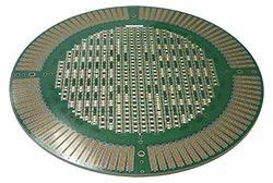
What is Gold Plating in PCBs?
Gold plating in PCBs involves depositing a thin layer of gold onto the surface of the copper traces and pads. This process is performed to enhance the electrical conductivity, corrosion resistance, and solderability of the PCB. Gold is an excellent choice for plating due to its high conductivity, resistance to oxidation, and compatibility with various soldering techniques.
Benefits of Gold Plating PCBs
- Enhanced conductivity: Gold is an excellent conductor of electricity, ensuring minimal signal loss and improved performance of the PCB.
- Corrosion resistance: Gold is highly resistant to corrosion, protecting the underlying copper from oxidation and ensuring long-term reliability.
- Improved solderability: Gold-plated surfaces facilitate easier and more reliable soldering of components to the PCB.
- Reduced contact resistance: Gold plating minimizes contact resistance between the PCB and connected components, improving signal integrity.
- Extended product life: The protective properties of gold plating contribute to the longevity of the PCB and its components.
Gold Plating Methods for PCBs
There are several methods used for gold plating PCBs, each with its own advantages and considerations. The choice of method depends on factors such as the desired thickness of the gold layer, the complexity of the PCB design, and production volume.
Electroless Gold Plating
Electroless gold plating, also known as immersion gold plating, is a chemical process that deposits a thin layer of gold onto the copper surface without the use of an external electrical current. This method involves the following steps:
- Surface preparation: The PCB is cleaned and conditioned to ensure proper adhesion of the gold layer.
- Immersion: The PCB is immersed in a gold plating solution containing a gold salt and a reducing agent.
- Chemical reaction: The reducing agent in the solution causes the gold ions to be reduced and deposited onto the copper surface.
- Rinsing and drying: The PCB is rinsed with water to remove any excess plating solution and then dried.
Advantages of electroless gold plating:
– Uniform coverage, even on complex PCB designs
– No electrical current required
– Suitable for small-scale production and prototyping
Disadvantages of electroless gold plating:
– Limited control over the thickness of the gold layer
– Slower plating process compared to electrolytic methods
Electrolytic Gold Plating
Electrolytic gold plating involves the use of an external electrical current to deposit gold onto the copper surface of the PCB. This method offers more control over the thickness of the gold layer and is suitable for high-volume production. The process involves the following steps:
- Surface preparation: The PCB is cleaned and conditioned to ensure proper adhesion of the gold layer.
- Anode and cathode setup: The PCB is connected as the cathode, while a gold anode is used as the source of gold ions.
- Electrolytic bath: The PCB and anode are immersed in an electrolytic bath containing a gold plating solution.
- Current application: An electrical current is applied, causing the gold ions to be attracted to the PCB surface and deposited as a thin layer.
- Rinsing and drying: The PCB is rinsed with water to remove any excess plating solution and then dried.
Advantages of electrolytic gold plating:
– Precise control over the thickness of the gold layer
– Faster plating process compared to electroless methods
– Suitable for high-volume production
Disadvantages of electrolytic gold plating:
– Requires an external electrical current source
– May have limitations in plating complex PCB designs

Gold Plating Thickness and Specifications
The thickness of the gold layer on a PCB is a critical factor in determining its performance and durability. The choice of gold plating thickness depends on the specific application and requirements of the PCB.
Common Gold Plating Thicknesses
| Thickness (µin) | Thickness (µm) | Application |
|---|---|---|
| 5-15 | 0.13-0.38 | Low-cost consumer electronics |
| 15-30 | 0.38-0.76 | General-purpose electronics |
| 30-50 | 0.76-1.27 | High-reliability and military applications |
| 50-100 | 1.27-2.54 | Extreme environments and aerospace |
Gold Plating Specifications
When specifying gold plating for PCBs, several factors should be considered:
- Gold purity: The purity of the gold used for plating, typically expressed as a percentage (e.g., 99.9% pure gold).
- Plating thickness: The desired thickness of the gold layer, usually measured in microinches (µin) or micrometers (µm).
- Adhesion: The ability of the gold layer to adhere to the underlying copper surface, often tested using a tape test or a scratch test.
- Porosity: The presence of tiny pores or voids in the gold layer, which can affect its protective properties and durability.
- Solderability: The ease with which components can be soldered to the gold-plated surface, assessed using wetting balance tests or spread tests.

Best Practices for Gold Plating PCBs
To ensure optimal results and long-term reliability of gold-plated PCBs, consider the following best practices:
- Surface preparation: Thoroughly clean and condition the PCB surface before gold plating to ensure proper adhesion and minimize defects.
- Plating thickness: Choose an appropriate gold plating thickness based on the specific application and environmental requirements of the PCB.
- Quality control: Implement strict quality control measures, including visual inspections, thickness measurements, and adhesion tests, to ensure consistent and reliable gold plating.
- Handling and storage: Handle gold-plated PCBs with care to avoid scratches or contamination, and store them in a clean, dry environment to maintain their integrity.
- Soldering considerations: Use compatible soldering techniques and materials when working with gold-plated PCBs to ensure reliable connections and avoid damage to the gold layer.

Frequently Asked Questions (FAQ)
-
Q: What are the advantages of gold plating over other plating materials for PCBs?
A: Gold plating offers several advantages over other materials, including excellent conductivity, corrosion resistance, solderability, and durability. These properties make gold an ideal choice for high-reliability and long-lasting PCBs. -
Q: How does the thickness of the gold plating affect the performance of a PCB?
A: The thickness of the gold plating influences the PCB’s performance in terms of conductivity, protection against corrosion, and durability. Thicker gold layers provide better protection and reliability, but also increase the cost of the PCB. The choice of thickness depends on the specific application and environmental factors. -
Q: Can gold-plated PCBs be reworked or repaired?
A: Yes, gold-plated PCBs can be reworked or repaired, but special care must be taken to avoid damaging the gold layer. Proper soldering techniques and compatible materials should be used to ensure reliable repairs and minimize the risk of contamination or delamination of the gold layer. -
Q: How does the gold plating process affect the lead time for PCB manufacturing?
A: The gold plating process can add to the overall lead time for PCB manufacturing, as it requires additional steps and processing time. The specific impact on lead time depends on factors such as the chosen plating method, the complexity of the PCB design, and the production volume. It is important to factor in the gold plating process when planning PCB production schedules. -
Q: Are there any environmental concerns associated with gold plating PCBs?
A: Gold plating processes can have environmental impacts due to the use of chemicals and the generation of waste. Responsible PCB manufacturers employ eco-friendly practices, such as properly handling and disposing of plating solutions, minimizing water usage, and implementing waste reduction strategies. Adhering to environmental regulations and using green technologies can help mitigate the environmental impact of gold plating PCBs.
Conclusion
Gold plating is a critical process in the manufacturing of high-quality and reliable PCBs. By depositing a thin layer of gold onto the copper surfaces of the PCB, manufacturers can enhance the conductivity, corrosion resistance, and solderability of the board. Understanding the different gold plating methods, thickness specifications, and best practices is essential for ensuring optimal performance and longevity of gold-plated PCBs. As the electronics industry continues to advance, the demand for gold-plated PCBs is likely to grow, driven by the need for high-reliability components in increasingly complex and demanding applications.


Leave a Reply