Introduction to PCB Prototyping
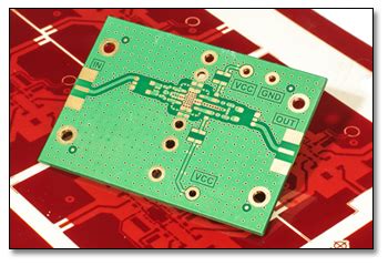
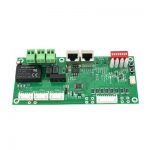
PCB prototyping is the process of creating a preliminary version of a printed circuit board (PCB) for testing and evaluation purposes before going into full-scale production. It allows designers and engineers to validate their designs, check for any errors or issues, and make necessary modifications before committing to a large production run.
Key benefits of PCB prototyping:
- Cost-effective: Prototyping helps identify and rectify design flaws early, avoiding expensive mistakes in mass production.
- Time-saving: Prototypes can be quickly fabricated and tested, reducing overall development time.
- Design optimization: Prototyping allows for iterative improvements and refinements to the PCB design.
Differences between PCB Prototyping and Full Spec Standard PCB Production
While both PCB prototyping and full spec standard PCB production involve the fabrication of printed circuit boards, there are several key differences between the two processes:
Purpose
- PCB Prototyping: The primary purpose of prototyping is to test and validate the PCB design before mass production. It allows designers to identify and fix any issues, ensuring the final product meets the required specifications and functions as intended.
- Full Spec Standard PCB Production: The goal of standard PCB production is to manufacture large quantities of PCBs that have already been tested and validated through the prototyping phase. The focus is on producing high-quality, reliable boards in a cost-effective manner.
Quantity
- PCB Prototyping: Prototyping typically involves producing a small number of boards, usually ranging from a single unit to a few dozen. The exact quantity depends on the complexity of the design and the extent of testing required.
- Full Spec Standard PCB Production: Standard PCB production deals with much larger quantities, often ranging from hundreds to thousands of units per batch. The higher volumes allow for economies of scale and reduced per-unit costs.
Lead Time
- PCB Prototyping: Prototype PCBs can often be fabricated and delivered within a shorter timeframe compared to standard production. Many PCB prototyping services offer quick-turn options, with lead times ranging from a few days to a couple of weeks.
- Full Spec Standard PCB Production: Due to the larger quantities involved and the need for more extensive quality control measures, standard PCB production typically has longer lead times. Depending on the complexity of the design and the manufacturer’s capacity, lead times can range from several weeks to a few months.
Cost
- PCB Prototyping: The cost per unit for prototype PCBs is generally higher than that of standard production boards. This is due to the lower quantities, faster turnaround times, and the additional setup and tooling costs associated with prototyping.
- Full Spec Standard PCB Production: With larger production volumes, the cost per unit for standard PCBs is significantly lower than that of prototypes. The higher quantities allow for more efficient use of materials and resources, resulting in reduced manufacturing costs.
Design Flexibility
- PCB Prototyping: Prototyping allows for greater design flexibility, as changes and modifications can be easily incorporated based on the results of testing and evaluation. Designers can experiment with different layouts, components, and materials to optimize the PCB’s performance.
- Full Spec Standard PCB Production: Once a design has been finalized and validated through prototyping, there is less room for design changes in standard production. Any significant modifications may require additional prototyping and testing, which can impact the production timeline and costs.
Quality Control
- PCB Prototyping: Quality control measures in prototyping are typically less stringent compared to standard production. The focus is on quickly fabricating functional boards for testing and evaluation, rather than ensuring strict adherence to all manufacturing standards.
- Full Spec Standard PCB Production: Standard PCB production involves rigorous quality control procedures to ensure that every board meets the required specifications and standards. This includes automated optical inspection (AOI), electrical testing, and other quality assurance measures to minimize defects and maintain consistency across the entire production run.
PCB Prototyping Techniques
There are several techniques used in PCB prototyping, each with its own advantages and limitations:
Breadboarding
Breadboarding is a quick and easy way to prototype simple electronic circuits without the need for soldering. It involves using a breadboard, which is a reusable plastic board with a matrix of interconnected sockets. Components can be inserted into the sockets and connected using jumper wires to create a temporary circuit.
Advantages:
– Quick and easy to set up and modify
– No soldering required
– Ideal for simple circuits and basic proof-of-concept testing
Limitations:
– Not suitable for complex or high-frequency circuits
– Limited component compatibility
– Prone to loose connections and electrical noise
Perfboard Prototyping
Perfboard prototyping involves using a perforated board with a grid of holes to manually solder components and create a more permanent prototype. The components are placed on one side of the board and soldered on the other side, with wires used to make the necessary connections.
Advantages:
– More durable than breadboarding
– Allows for more complex circuits
– Provides a more realistic representation of the final PCB layout
Limitations:
– Requires soldering skills
– Time-consuming for larger or more intricate designs
– Limited routing options compared to a custom-designed PCB
PCB Milling
PCB milling is a subtractive manufacturing process that uses a computer-controlled milling machine to remove copper from a pre-fabricated copper-clad board. The milling machine follows a digital design file to create the desired circuit pattern, cutting away the unwanted copper and leaving the required traces and pads.
Advantages:
– Faster and more precise than manual prototyping methods
– Allows for the creation of double-sided and multi-layer boards
– Suitable for low-volume production and rapid prototyping
Limitations:
– Requires access to a PCB milling machine and associated software
– Limited to the capabilities of the milling machine (e.g., minimum trace width and spacing)
– Higher setup costs compared to breadboarding or perfboard prototyping
3D Printing
While not a traditional PCB prototyping method, 3D printing can be used to create custom enclosures, housings, and other mechanical components that integrate with the PCB. Some advanced 3D printing techniques, such as conductive ink printing, can even be used to create basic circuit patterns.
Advantages:
– Allows for rapid prototyping of custom mechanical parts
– Enables the creation of complex geometries and shapes
– Can be used in conjunction with other PCB prototyping methods
Limitations:
– Limited electrical functionality compared to traditional PCB prototyping methods
– Requires access to a 3D printer and compatible materials
– Post-processing may be necessary for smooth finishes and accurate dimensions

Choosing the Right PCB Prototyping Method
When selecting a PCB prototyping method, consider the following factors:
-
Circuit complexity: Simple circuits can be easily prototyped using breadboarding or perfboard, while more complex designs may require PCB milling or custom fabrication.
-
Required durability: If the prototype needs to withstand extensive handling or testing, a more permanent solution like perfboard or milled PCBs may be preferable.
-
Time constraints: Breadboarding and perfboard prototyping are typically faster for smaller designs, while PCB milling and custom fabrication may be quicker for larger or more complex circuits.
-
Budget: Breadboarding and perfboard prototyping are generally the most cost-effective options, while PCB milling and custom fabrication have higher setup costs but may be more economical for larger quantities.
-
Available resources: Consider the tools, equipment, and skills available to you. If you have access to a PCB milling machine or 3D printer, these methods may be more feasible than if you had to outsource the work.
Full Spec Standard PCB Production Process
Once a PCB design has been finalized and validated through prototyping, it can move into full spec standard production. The standard PCB production process typically involves the following steps:
-
Design review: The PCB design files are reviewed by the manufacturer to ensure they meet all the necessary specifications and requirements for production.
-
Tooling and setup: The manufacturer prepares the required tooling, such as stencils and jigs, and sets up the production line according to the design specifications.
-
Material preparation: The raw materials, including the copper-clad boards, laminates, and prepregs, are cut to the required sizes and shapes.
-
Patterning: The circuit pattern is transferred onto the copper-clad board through a process of etching, plating, or a combination of both. This involves applying a photoresist layer, exposing it to light through a photomask, and developing the pattern.
-
Drilling: Holes are drilled into the board for through-hole components, vias, and mounting points using computer-controlled drilling machines.
-
Plating: The holes and exposed copper surfaces are plated with a conductive material, typically copper, to improve conductivity and protect against corrosion.
-
Solder mask application: A solder mask layer is applied to the board to insulate and protect the copper traces, leaving only the desired areas exposed for soldering.
-
Silkscreen printing: Text, logos, and other markings are printed onto the board using a silkscreen process to aid in assembly and identification.
-
Surface finishing: The exposed copper areas are coated with a protective finish, such as HASL (Hot Air Solder Leveling), ENIG (Electroless Nickel Immersion Gold), or OSP (Organic Solderability Preservative), to improve solderability and prevent oxidation.
-
Singulation: The individual PCBs are cut and separated from the larger panel using a routing or punching process.
-
Quality control: The finished PCBs undergo rigorous quality control checks, including automated optical inspection (AOI), electrical testing, and visual inspections, to ensure they meet the required specifications and standards.
-
Packaging and shipping: The PCBs are packaged according to the customer’s requirements and shipped to their destination.
Advantages of Full Spec Standard PCB Production
Full spec standard PCB production offers several advantages over prototyping:
-
Cost-effectiveness: With larger production volumes, the cost per unit is significantly lower than that of prototypes. This makes standard production a more economical choice for high-volume applications.
-
Consistency: Standard production processes ensure that every PCB is manufactured to the same specifications and quality standards, resulting in a more consistent and reliable end product.
-
Scalability: Once a design has been validated through prototyping, standard production allows for easy scaling to meet increased demand or future product iterations.
-
Enhanced quality control: Standard production involves rigorous quality control measures, including automated inspections and testing, to minimize defects and ensure that every board meets the required specifications.
-
Access to advanced manufacturing capabilities: Full-scale PCB manufacturers often have access to more advanced equipment and processes, such as multi-layer fabrication, fine-pitch components, and specialized surface finishes, which may not be available or cost-effective for prototyping.
Challenges in Full Spec Standard PCB Production
While full spec standard PCB production offers many benefits, there are also some challenges to consider:
-
Higher upfront costs: Setting up a standard production run requires significant investment in tooling, materials, and setup costs. This can be a barrier for smaller companies or those with limited budgets.
-
Longer lead times: Due to the larger quantities involved and the need for extensive quality control, standard production lead times are typically longer than those for prototyping.
-
Less flexibility for design changes: Once a design has been finalized and moved into standard production, making changes can be costly and time-consuming. Any significant modifications may require additional prototyping and validation before being implemented in the production run.
-
Minimum order quantities: Many PCB manufacturers have minimum order quantity (MOQ) requirements for standard production runs. This can be a challenge for companies with lower volume needs or those looking to test the market before committing to a larger production run.
-
Communication and collaboration: Effective communication and collaboration between the design team and the PCB manufacturer are essential for successful standard production. Any misunderstandings or miscommunications can lead to delays, quality issues, or additional costs.
Conclusion
PCB prototyping and full spec standard PCB production are two essential processes in the development and manufacturing of electronic devices. While prototyping focuses on testing and validating designs quickly and cost-effectively, standard production aims to manufacture high-quality, reliable boards in larger quantities.
Understanding the differences between these two processes, as well as the various prototyping techniques available, can help designers and engineers make informed decisions when developing and scaling their PCB-based products. By leveraging the strengths of both prototyping and standard production, companies can bring innovative, high-quality electronic devices to market more efficiently and effectively.
FAQ
- What is the main purpose of PCB prototyping?
-
The main purpose of PCB prototyping is to test and validate the PCB design before moving into full-scale production. It allows designers to identify and fix any issues, ensuring the final product meets the required specifications and functions as intended.
-
How does the cost per unit differ between PCB prototyping and standard production?
-
The cost per unit for prototype PCBs is generally higher than that of standard production boards due to the lower quantities, faster turnaround times, and additional setup and tooling costs. In contrast, the cost per unit for standard PCBs is significantly lower because of the larger production volumes and more efficient use of materials and resources.
-
What are some common PCB prototyping techniques?
-
Common PCB prototyping techniques include breadboarding, perfboard prototyping, PCB milling, and 3D printing. Each method has its own advantages and limitations, and the choice depends on factors such as circuit complexity, required durability, time constraints, budget, and available resources.
-
What quality control measures are involved in full spec standard PCB production?
-
Full spec standard PCB production involves rigorous quality control procedures, including automated optical inspection (AOI), electrical testing, and visual inspections. These measures help ensure that every board meets the required specifications and standards, minimizing defects and maintaining consistency across the entire production run.
-
What are some challenges associated with full spec standard PCB production?
- Some challenges in full spec standard PCB production include higher upfront costs for tooling and setup, longer lead times compared to prototyping, less flexibility for design changes, minimum order quantity requirements, and the need for effective communication and collaboration between the design team and the PCB manufacturer.
Leave a Reply