Introduction to Flexible PCBs
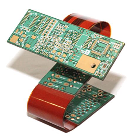
Flexible printed circuit boards (PCBs) have revolutionized the electronics industry by providing a versatile and adaptable solution for various applications. Unlike traditional rigid PCBs, flexible PCBs can bend, twist, and fold without compromising their electrical functionality. This unique characteristic makes them ideal for use in compact devices, Wearable Technology, and applications requiring movement or flexibility.
In this comprehensive guide, we will explore the world of flexible PCBs and provide you with a step-by-step tutorial on how to create your own DIY flexible PCB. We will cover everything from the basics of flexible PCBs to the materials and tools required, design considerations, and the manufacturing process.
What is a Flexible PCB?
A flexible PCB, also known as a flex circuit or flexible printed wiring board, is a type of printed circuit board that consists of a thin, flexible substrate with conductive traces and components mounted on it. The substrate is typically made of polyimide or other flexible materials, allowing the PCB to bend and conform to various shapes and configurations.
Flexible PCBs offer several advantages over rigid PCBs:
- Flexibility: Flexible PCBs can bend and twist, making them suitable for applications where flexibility is required.
- Lightweight: Due to their thin substrate and minimal components, flexible PCBs are often lighter than rigid PCBs.
- Space-saving: Flexible PCBs can be folded or rolled, allowing for more compact designs and efficient use of space.
- Durability: Flexible PCBs can withstand repeated bending and flexing without breaking or losing electrical connectivity.
- Improved signal integrity: The close proximity of components and shorter trace lengths in flexible PCBs can lead to better signal integrity and reduced noise.
Applications of Flexible PCBs
Flexible PCBs find applications in various industries and devices, including:
- Wearable technology: Smartwatches, fitness trackers, and medical devices.
- Consumer electronics: Smartphones, tablets, cameras, and portable gaming devices.
- Automotive industry: Dashboard displays, sensors, and vehicle electronics.
- Aerospace and defense: Avionics, satellites, and military equipment.
- Medical devices: Implantable devices, diagnostic tools, and monitoring systems.
Materials and Tools Required
Before diving into the DIY flexible PCB manufacturing process, let’s take a look at the materials and tools you’ll need.
Materials
- Flexible substrate (e.g., polyimide film)
- Copper foil
- Adhesive (e.g., acrylic or epoxy)
- Photoresist film
- Etchant solution (e.g., ferric chloride)
- Solder mask ink
- Solder paste
- Components for your circuit
Tools
- Computer with PCB design software
- Laser printer or photoplotter
- UV exposure unit
- Developing tray
- Etching tank
- Drill or punching tool
- Soldering iron
- Multimeter
- Safety equipment (gloves, goggles, etc.)

Designing Your Flexible PCB
The first step in creating your DIY flexible PCB is designing the circuit. This involves creating a schematic diagram and converting it into a PCB layout.
Schematic Design
- Use PCB design software (e.g., KiCad, Eagle, or Altium Designer) to create your schematic diagram.
- Define the components and their connections based on your circuit requirements.
- Assign appropriate footprints to each component.
- Verify the schematic for errors and inconsistencies.
PCB Layout
- Convert the schematic into a PCB layout using the design software.
- Define the board outline and dimensions, considering the flexibility and bending requirements.
- Place components strategically to optimize space and minimize trace lengths.
- Route the traces, ensuring proper width and spacing for flexibility and signal integrity.
- Add copper pours for shielding and heat dissipation, if necessary.
- Generate Gerber files for manufacturing.
Design Considerations for Flexible PCBs
When designing a flexible PCB, keep the following considerations in mind:
- Bend radius: Ensure that the components and traces can withstand the required bend radius without damage.
- Strain relief: Incorporate strain relief features, such as stiffeners or anchors, to prevent excessive stress on components and connections.
- Trace width and spacing: Use appropriate trace widths and spacing to maintain flexibility and minimize the risk of cracking or breaking.
- Component placement: Place components strategically to minimize stress during bending and to optimize space utilization.
- Material selection: Choose a flexible substrate and adhesive that can withstand the expected environmental conditions and mechanical stresses.

Manufacturing Process
Once your flexible PCB design is complete, it’s time to start the manufacturing process. Follow these steps to create your DIY flexible PCB:
Step 1: Printing the Circuit Pattern
- Print the circuit pattern onto a transparency film using a laser printer or photoplotter.
- Ensure that the printed pattern is sharp, well-defined, and has the correct dimensions.
Step 2: Laminating the Flexible Substrate
- Clean the flexible substrate (e.g., polyimide film) to remove any dirt or contaminants.
- Laminate the copper foil onto the substrate using adhesive and a laminating machine.
- Ensure proper adhesion between the copper foil and the substrate.
Step 3: Applying Photoresist
- Apply a layer of photoresist film onto the copper-laminated substrate.
- Use a laminating machine to ensure uniform coverage and adhesion of the photoresist.
Step 4: UV Exposure
- Place the transparency film with the circuit pattern onto the photoresist-coated substrate.
- Expose the assembly to UV light using a UV exposure unit for the recommended time.
- The UV light will harden the exposed portions of the photoresist, while the unexposed portions remain soluble.
Step 5: Developing
- Immerse the exposed substrate in a developing solution to remove the unexposed portions of the photoresist.
- Rinse the substrate with water and dry it thoroughly.
Step 6: Etching
- Prepare the etching solution (e.g., ferric chloride) according to the manufacturer’s instructions.
- Immerse the developed substrate in the etching solution.
- The etching solution will remove the copper that is not protected by the hardened photoresist, leaving only the desired circuit pattern.
- Rinse the etched substrate with water and dry it.
Step 7: Removing Photoresist
- Use a photoresist stripper solution to remove the remaining hardened photoresist from the substrate.
- Rinse the substrate with water and dry it.
Step 8: Applying Solder Mask
- Apply a layer of solder mask ink onto the etched substrate, covering the areas where soldering is not required.
- Cure the solder mask using UV light or heat, according to the manufacturer’s instructions.
Step 9: Drilling and Cutting
- Drill or punch any necessary holes for component mounting or connections.
- Cut the flexible PCB to the desired shape and size using scissors or a cutting tool.
Step 10: Component Placement and Soldering
- Apply solder paste to the pads where components will be placed.
- Place the components onto the pads, ensuring proper alignment.
- Use a soldering iron to solder the components securely to the pads.
- Clean any excess solder or flux residue.
Step 11: Testing and Verification
- Use a multimeter to test the continuity and functionality of the assembled flexible PCB.
- Verify that all components are correctly soldered and that there are no short circuits or open connections.

Tips and Tricks for Successful Flexible PCB Manufacturing
- Use high-quality materials to ensure the best results and reliability.
- Maintain a clean and organized workspace to avoid contamination and errors.
- Follow the manufacturer’s instructions for each step of the process, including exposure times, etching durations, and curing temperatures.
- Practice proper safety measures, such as wearing gloves and goggles, when handling chemicals and tools.
- Double-check your design and connections before proceeding with the manufacturing process to avoid costly mistakes.
- Start with simple designs and gradually increase complexity as you gain experience and confidence.
- Seek guidance from experienced professionals or online resources if you encounter any challenges or have questions.
Troubleshooting Common Issues
Despite following the manufacturing process carefully, you may encounter some issues along the way. Here are a few common problems and their potential solutions:
- Incomplete etching: If the etching process is incomplete, resulting in unwanted copper traces, increase the etching time or replace the etching solution.
- Over-etching: If the etching process removes too much copper, reducing the trace widths, decrease the etching time or dilute the etching solution.
- Poor adhesion between layers: Ensure that the surfaces are clean and free from contaminants before laminating. Apply adequate pressure and heat during the lamination process.
- Solder bridging: Use a fine-tipped soldering iron and apply solder sparingly. Clean any excess solder using a solder wick or desoldering pump.
- Component misalignment: Use a magnifying glass or microscope to ensure accurate component placement. Double-check the orientation and alignment before soldering.
Frequently Asked Questions (FAQ)
-
Can I use any type of flexible substrate for my DIY flexible PCB?
While polyimide film is the most common substrate for flexible PCBs, you can also use other materials such as polyester or PET. However, ensure that the substrate is compatible with the adhesive and can withstand the manufacturing process and intended application. -
What is the minimum bend radius for a flexible PCB?
The minimum bend radius depends on various factors, including the substrate material, copper thickness, and component placement. As a general rule, the bend radius should be at least 6 times the thickness of the PCB to avoid cracking or damaging the traces and components. -
Can I create multilayer flexible PCBs using the DIY method?
Yes, it is possible to create multilayer flexible PCBs using the DIY method. However, it requires additional steps such as aligning and laminating multiple layers together. It is recommended to start with single-layer designs and gradually progress to multilayer boards as you gain experience. -
How do I choose the right trace width and spacing for my flexible PCB?
The trace width and spacing depend on the current requirements, signal integrity, and flexibility needs of your design. As a general guideline, use wider traces for higher current-carrying capacity and narrower traces for increased flexibility. Ensure adequate spacing between traces to prevent short circuits and maintain signal integrity. -
Can I reuse the etching solution for multiple PCBs?
Yes, you can reuse the etching solution for multiple PCBs as long as it remains effective. However, the etching process will gradually deplete the solution, reducing its strength over time. Monitor the etching speed and replace the solution when it becomes significantly slower or less effective.
Conclusion
Creating your own DIY flexible PCB can be a rewarding and educational experience. By following the step-by-step manufacturing process and considering the design guidelines, you can bring your flexible circuit ideas to life.
Remember to prioritize safety, use high-quality materials, and start with simple designs before tackling more complex projects. With practice and persistence, you’ll be able to create professional-quality flexible PCBs in your own workspace.
Embrace the flexibility and versatility offered by flexible PCBs and unleash your creativity in the world of electronics. Happy PCB making!


Leave a Reply