Introduction to Flexible PCBs
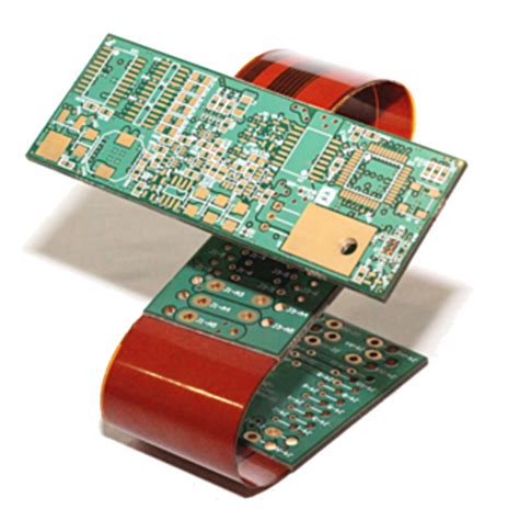
Flexible PCBs, also known as flex circuits, are a type of printed circuit board that consists of a thin, flexible substrate made of polyimide or other flexible materials. Unlike traditional rigid PCBs, flexible PCBs can bend, twist, and conform to various shapes and sizes, making them ideal for applications that require compact packaging, lightweight design, and enhanced reliability.
Key Features of Flexible PCBs
-
Flexibility: The most distinguishing feature of flexible PCBs is their ability to bend and flex without compromising the integrity of the circuit. This flexibility allows for greater design freedom and enables the integration of electronic components into tight spaces and complex geometries.
-
Lightweight: Flexible PCBs are significantly lighter than their rigid counterparts, making them an attractive option for satellite applications where every gram counts. The reduced weight helps to minimize the overall mass of the satellite, reducing launch costs and improving fuel efficiency.
-
High Reliability: Flexible PCBs offer superior reliability compared to rigid PCBs, especially in harsh environments such as those encountered in space. The flexible nature of the substrate allows for better stress distribution and reduces the risk of cracking or delamination due to thermal cycling and vibration.
-
Improved Signal Integrity: The thin, compact design of flexible PCBs minimizes the distance between components, reducing signal loss and improving signal integrity. This is particularly important in satellite applications where high-speed data transmission and precise signal control are critical.
Advantages of Flexible PCBs in Satellite Applications
Space Savings and Compact Packaging
One of the primary reasons why flexible PCBs are the best choice for satellite applications is their ability to save space and enable compact packaging. Satellites are inherently limited in terms of available space, and every component must be carefully designed to maximize efficiency and minimize volume.
Flexible PCBs can be bent, folded, and shaped to fit into tight spaces and conform to the contours of the satellite structure. This allows for more efficient use of the available space, enabling the integration of more components and functionality within a smaller footprint.
| Component | Rigid PCB | Flexible PCB |
|---|---|---|
| Board Thickness | 1.6 mm | 0.2 mm |
| Minimum Bend Radius | N/A | 6x thickness |
| Typical Weight (per dm^2^) | 30 g | 8 g |
As shown in the table above, flexible PCBs offer significant advantages in terms of thickness, bend radius, and weight compared to rigid PCBs. These properties make them ideal for satellite applications where space is at a premium and every gram counts.
Reduced Weight and Launch Costs
In addition to space savings, the lightweight nature of flexible PCBs is another crucial factor that makes them the best choice for satellite applications. Satellites are extremely weight-sensitive, and every component must be carefully selected to minimize the overall mass of the spacecraft.
Flexible PCBs are significantly lighter than rigid PCBs, with a typical weight of around 8 grams per square decimeter compared to 30 grams for rigid boards. This weight reduction can have a substantial impact on the overall mass of the satellite, especially when considering the numerous PCBs required for various subsystems.
The reduced weight of flexible PCBs directly translates to lower launch costs. Launching a satellite into orbit is an extremely expensive endeavor, with costs ranging from tens of millions to hundreds of millions of dollars. Every kilogram of payload mass contributes to the overall launch cost, making weight reduction a top priority for satellite manufacturers.
By utilizing flexible PCBs, satellite designers can significantly reduce the weight of the electronic components, leading to lower launch costs and improved fuel efficiency. This cost savings can be reinvested into additional payload capacity, enhanced functionality, or extended mission durations.
Enhanced Reliability in Harsh Environments
Satellites operate in the harsh environment of space, exposed to extreme temperatures, radiation, and vibration. These conditions can take a toll on electronic components, leading to failures and compromised mission objectives. Flexible PCBs offer enhanced reliability in these challenging environments, making them the best choice for satellite applications.
The flexible nature of the substrate allows for better stress distribution and reduces the risk of cracking or delamination due to thermal cycling and vibration. Unlike rigid PCBs, which can develop cracks and fractures under stress, flexible PCBs can absorb and dissipate mechanical stresses more effectively.
| Environmental Factor | Rigid PCB | Flexible PCB |
|---|---|---|
| Temperature Range | -55°C to +125°C | -200°C to +200°C |
| Thermal Cycling | Limited cycles before failure | Withstands >1000 cycles |
| Vibration Resistance | Prone to cracking and fracture | Absorbs and dissipates vibration energy |
As shown in the table above, flexible PCBs offer superior performance in terms of temperature range, thermal cycling, and vibration resistance compared to rigid PCBs. These properties make them ideal for satellite applications where reliability is of utmost importance.
Furthermore, flexible PCBs can be designed with additional features to enhance their reliability in space. For example, the use of polyimide substrates provides excellent resistance to radiation and outgassing, while the incorporation of shielding layers can protect sensitive components from electromagnetic interference.
Improved Signal Integrity and High-Speed Data Transmission
Satellite applications often require high-speed data transmission and precise signal control to ensure effective communication and data processing. Flexible PCBs offer improved signal integrity and high-speed data transmission capabilities compared to rigid PCBs, making them the best choice for these demanding applications.
The thin, compact design of flexible PCBs minimizes the distance between components, reducing signal loss and improving signal integrity. The shorter signal paths and reduced parasitic capacitance and inductance enable faster signal propagation and cleaner waveforms.
| Parameter | Rigid PCB | Flexible PCB |
|---|---|---|
| Dielectric Constant (Dk) | 4.5 | 3.5 |
| Dissipation Factor (Df) | 0.02 | 0.002 |
| Propagation Delay (ps/inch) | 180 | 140 |
As shown in the table above, flexible PCBs have a lower dielectric constant and dissipation factor compared to rigid PCBs, resulting in reduced signal loss and improved signal integrity. The lower propagation delay also enables faster signal transmission, which is crucial for high-speed data communication in satellite applications.
Flexible PCBs can also be designed with controlled impedance traces and differential pairs to further enhance signal integrity and minimize crosstalk. The use of advanced materials, such as low-loss dielectrics and high-conductivity copper, contributes to the superior performance of flexible PCBs in high-speed applications.

Design Considerations for Flexible PCBs in Satellite Applications
Material Selection
When designing flexible PCBs for satellite applications, material selection is a critical consideration. The choice of substrate material, conductor material, and cover layer material can significantly impact the performance, reliability, and durability of the flexible PCB.
| Material | Properties |
|---|---|
| Polyimide (PI) | High temperature resistance, excellent mechanical strength |
| Polyester (PET) | Lower cost, good flexibility, limited temperature range |
| Copper | High conductivity, standard conductor material |
| Aluminum | Lightweight, used for shielding and heat dissipation |
| Coverlay | Insulation, protection, and mechanical reinforcement |
Polyimide (PI) is the most commonly used substrate material for flexible PCBs in satellite applications due to its excellent thermal stability, mechanical strength, and resistance to radiation and outgassing. PI can withstand temperatures ranging from -200°C to +200°C, making it suitable for the extreme temperature variations encountered in space.
Copper is the standard conductor material used in flexible PCBs, offering high conductivity and compatibility with various manufacturing processes. In some cases, aluminum may be used as a lightweight alternative for shielding layers or heat dissipation.
The choice of cover layer material is also important, as it provides insulation, protection, and mechanical reinforcement to the flexible PCB. Common cover layer materials include polyimide, acrylic, and epoxy-based laminates.
Bend Radius and Flexibility Requirements
When designing flexible PCBs for satellite applications, it is crucial to consider the bend radius and flexibility requirements of the specific application. The bend radius refers to the minimum radius at which the flexible PCB can be bent without causing damage or compromising its functionality.
| Bend Radius | Recommended Minimum |
|---|---|
| Single Bend | 6x PCB thickness |
| Dynamic Bend | 12x PCB thickness |
As a general guideline, the minimum bend radius for a single bend should be at least six times the thickness of the flexible PCB. For dynamic or repeated bending, the minimum bend radius should be increased to twelve times the thickness to ensure long-term reliability.
Designers must also consider the flexibility requirements of the application, such as the number of bending cycles, the range of motion, and the expected lifespan of the flexible PCB. These factors will influence the choice of materials, the thickness of the substrate and conductors, and the overall layout of the PCB.
Shielding and Grounding Techniques
Effective shielding and grounding techniques are essential for flexible PCBs in satellite applications to ensure electromagnetic compatibility (EMC) and protect sensitive components from interference.
| Shielding Technique | Description |
|---|---|
| Ground Planes | Continuous conductive layer for shielding and grounding |
| Shielding Layers | Additional layers for enhanced shielding effectiveness |
| Shielded Connectors | Connectors with integrated shielding features |
The use of ground planes is a common technique in flexible PCB design, providing a continuous conductive layer that serves as a shield against electromagnetic interference (EMI) and a reference plane for grounding. Ground planes can be incorporated as a dedicated layer or as a partitioned area on a signal layer.
In addition to ground planes, flexible PCBs can include dedicated shielding layers to further enhance shielding effectiveness. These layers can be made of conductive materials such as copper or aluminum and are strategically placed to provide maximum coverage and protection.
Shielded connectors, such as coaxial or shielded ribbon connectors, are also important for maintaining shielding continuity and preventing interference at the interface between the flexible PCB and other components.
Proper grounding techniques, such as the use of ground vias, ground stitching, and low-impedance ground connections, are essential for ensuring a robust and effective grounding system in flexible PCBs for satellite applications.

Real-World Examples of Flexible PCBs in Satellite Applications
CubeSat Deployable Solar Arrays
CubeSats are small, modular satellites that have gained popularity in recent years due to their low cost and rapid development cycle. Flexible PCBs have been instrumental in enabling the design of deployable solar arrays for CubeSats, which are critical for power generation in space.
Flexible PCBs are used to create the interconnects between the solar cells and the satellite’s power management system. The flexibility of the PCB allows the solar array to be folded and stowed during launch and then deployed once the satellite is in orbit. This compact packaging enables CubeSats to maximize their power generation capabilities while minimizing the use of valuable space.
Satellite Communication Antennas
Flexible PCBs have also found applications in satellite communication antennas, particularly in the design of phased array antennas. Phased array antennas consist of multiple radiating elements that can be individually controlled to steer the antenna beam electronically.
Flexible PCBs are used to create the interconnects between the radiating elements and the control circuitry, allowing for a compact and lightweight design. The flexibility of the PCB enables the antenna to conform to the shape of the satellite, maximizing the available space and reducing the overall size of the antenna assembly.
Spacecraft Wiring Harnesses
Flexible PCBs are increasingly being used as an alternative to traditional wiring harnesses in spacecraft and satellite applications. Wiring harnesses are complex assemblies of cables and connectors that distribute power and signals throughout the spacecraft.
By replacing traditional wiring harnesses with flexible PCBs, designers can achieve significant weight and space savings, as well as improved reliability and reduced assembly time. Flexible PCBs can be designed to integrate multiple layers of conductors, eliminating the need for separate cables and connectors.
The use of flexible PCBs in spacecraft wiring harnesses also offers enhanced flexibility and vibration resistance compared to traditional cable assemblies, improving the overall reliability and durability of the system.

FAQs
Q1: What is a flexible PCB, and how does it differ from a rigid PCB?
A1: A flexible PCB, also known as a flex circuit, is a type of printed circuit board that consists of a thin, flexible substrate made of materials such as polyimide. Unlike rigid PCBs, which are made of a solid, inflexible substrate, flexible PCBs can bend, twist, and conform to various shapes and sizes. This flexibility allows for greater design freedom, compact packaging, and improved reliability in applications that require flexibility or have limited space.
Q2: Why are flexible PCBs particularly well-suited for satellite applications?
A2: Flexible PCBs are particularly well-suited for satellite applications for several reasons:
1. Space savings and compact packaging: Flexible PCBs can be bent, folded, and shaped to fit into tight spaces and conform to the contours of the satellite structure, enabling more efficient use of the available space.
2. Reduced weight: Flexible PCBs are significantly lighter than rigid PCBs, which is crucial for satellite applications where every gram counts. The reduced weight helps to minimize the overall mass of the satellite, reducing launch costs and improving fuel efficiency.
3. Enhanced reliability: Flexible PCBs offer superior reliability in the harsh environment of space, with better stress distribution and reduced risk of cracking or delamination due to thermal cycling and vibration.
4. Improved signal integrity: The thin, compact design of flexible PCBs minimizes the distance between components, reducing signal loss and improving signal integrity, which is critical for high-speed data transmission and precise signal control in satellite applications.
Q3: What are some of the key design considerations for flexible PCBs in satellite applications?
A3: When designing flexible PCBs for satellite applications, some of the key considerations include:
1. Material selection: Choosing the appropriate substrate material (e.g., polyimide), conductor material (e.g., copper), and cover layer material (e.g., coverlay) based on the specific requirements of the application, such as temperature range, mechanical strength, and radiation resistance.
2. Bend radius and flexibility requirements: Determining the minimum bend radius and flexibility requirements based on the specific application, considering factors such as the number of bending cycles, range of motion, and expected lifespan of the flexible PCB.
3. Shielding and grounding techniques: Incorporating effective shielding and grounding techniques, such as ground planes, shielding layers, and shielded connectors, to ensure electromagnetic compatibility and protect sensitive components from interference.
Q4: Can you provide some real-world examples of flexible PCBs being used in satellite applications?
A4: Yes, here are a few examples of flexible PCBs being used in satellite applications:
1. CubeSat deployable solar arrays: Flexible PCBs are used to create the interconnects between solar cells and the satellite’s power management system, allowing the solar array to be folded and stowed during launch and then deployed once the satellite is in orbit.
2. Satellite communication antennas: Flexible PCBs are used in phased array antennas to create interconnects between radiating elements and control circuitry, enabling a compact and lightweight design that can conform to the shape of the satellite.
3. Spacecraft wiring harnesses: Flexible PCBs are being used as an alternative to traditional wiring harnesses, offering weight and space savings, improved reliability, and reduced assembly time by integrating multiple layers of conductors and eliminating the need for separate cables and connectors.
Q5: How do flexible PCBs contribute to cost savings in satellite applications?
A5: Flexible PCBs contribute to cost savings in satellite applications in several ways:
1. Reduced launch costs: The lightweight nature of flexible PCBs helps to minimize the overall mass of the satellite, which directly translates to lower launch costs. Launching a satellite is extremely expensive, and every kilogram of payload mass contributes to the overall cost.
2. Space savings: Flexible PCBs enable more efficient use of the available space within a satellite, allowing for the integration of more components and functionality within a smaller footprint. This space savings can lead to reduced satellite size and complexity, further reducing costs.
3. Improved reliability: The enhanced reliability of flexible PCBs in the harsh environment of space reduces the risk of component failure and mission compromises, which can be extremely costly. By minimizing the need for redundancy and increasing the lifespan of the satellite, flexible PCBs contribute to long-term cost savings.
4. Simplified assembly: The use of flexible PCBs can simplify the assembly process of satellite electronic systems by reducing the number of interconnects and eliminating the


Leave a Reply