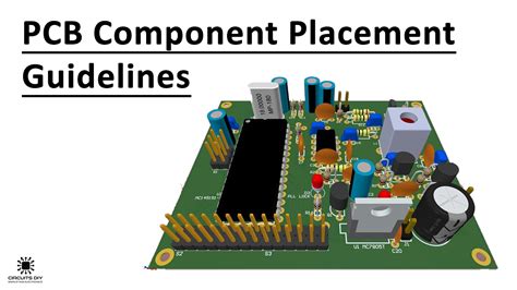
Introduction to PCB sensor placement
When designing a printed circuit board (PCB) that incorporates external sensors, proper placement is crucial for optimal performance and reliability. The location and orientation of the sensor on the PCB can significantly impact its functionality, accuracy, and overall system performance. In this article, we will explore the key considerations and best practices for placing external sensors on PCBs to be soldered.
Factors Affecting PCB Sensor Placement
Sensor Type and Characteristics
The type of sensor being used plays a significant role in determining its placement on the PCB. Different sensors have unique requirements in terms of physical size, mounting orientation, and environmental considerations. For example:
- Temperature sensors: These sensors should be placed away from heat-generating components and in an area that represents the average temperature of the system.
- Humidity sensors: Humidity sensors should be placed in a location that allows adequate airflow and avoids direct exposure to moisture or condensation.
- Accelerometers and gyroscopes: These sensors are sensitive to orientation and should be placed in a flat, stable position on the PCB.
PCB Layout and Component Placement
The overall layout of the PCB and the placement of other components can impact the optimal location for the external sensor. Consider the following factors:
- Proximity to other components: Ensure that the sensor is placed at a sufficient distance from other components to avoid interference or unintended interactions.
- Signal routing: Consider the signal routing requirements of the sensor and place it in a location that minimizes the length and complexity of the traces.
- Mechanical constraints: Take into account any mechanical constraints, such as mounting holes or enclosure requirements, when determining the sensor placement.
Environmental Factors
The environment in which the PCB will operate should also be considered when placing external sensors. Consider the following environmental factors:
- Temperature variations: If the PCB will be exposed to significant temperature variations, place the sensor in a location that minimizes thermal gradients and ensures accurate measurements.
- Vibration and shock: For applications subject to vibration or shock, place the sensor in a location that minimizes the impact of these forces on its performance.
- Electromagnetic interference (EMI): If the PCB will be exposed to EMI, place the sensor away from sources of interference and consider shielding techniques.

Best Practices for PCB Sensor Placement
Follow Manufacturer’s Recommendations
Always refer to the sensor manufacturer’s datasheet and application notes for specific placement guidelines. These resources often provide detailed information on the recommended mounting orientation, clearance requirements, and other considerations specific to the sensor.
Use Appropriate Mounting Techniques
The mounting technique used to attach the sensor to the PCB can affect its performance and reliability. Consider the following mounting techniques:
- Through-hole mounting: This technique involves inserting the sensor leads through holes in the PCB and soldering them on the opposite side. It provides a strong mechanical connection but may require additional space on the PCB.
- Surface-mount technology (SMT): SMT involves soldering the sensor directly onto the surface of the PCB. This technique allows for smaller footprints and automated assembly but may be more susceptible to mechanical stress.
Consider Thermal Management
For sensors that are sensitive to temperature variations or generate heat themselves, proper thermal management is essential. Consider the following techniques:
- Thermal isolation: Place the sensor away from heat-generating components and use thermal isolation techniques, such as air gaps or Thermal Pads, to minimize heat transfer.
- Heatsinks and cooling: If the sensor generates significant heat, consider using heatsinks or other cooling methods to dissipate the heat and maintain optimal operating temperatures.
Implement Shielding and Grounding
To minimize the impact of electromagnetic interference and ensure accurate sensor readings, implement appropriate shielding and grounding techniques:
- Shielding: Use shielding materials, such as metal enclosures or conductive tapes, to protect the sensor from external electromagnetic fields.
- Grounding: Ensure proper grounding of the sensor and the PCB to provide a stable reference point and minimize noise.
Conduct Testing and Validation
After placing the sensor on the PCB, conduct thorough testing and validation to ensure proper functionality and performance. This may include:
- Functional testing: Verify that the sensor operates as expected and provides accurate readings under various conditions.
- Environmental testing: Expose the PCB to the expected environmental conditions, such as temperature variations or vibration, to ensure the sensor’s performance remains within acceptable limits.
- Interference testing: Test the sensor’s susceptibility to electromagnetic interference and make necessary adjustments to the placement or shielding if required.

Sensor Placement Examples
To illustrate the principles of PCB sensor placement, let’s consider a few common scenarios:
Example 1: Temperature Sensor Placement
When placing a temperature sensor on a PCB, consider the following guidelines:
- Place the sensor away from heat-generating components, such as power regulators or processors.
- Ensure adequate airflow around the sensor to allow for accurate temperature measurements.
- If measuring the ambient temperature, place the sensor near the edge of the PCB or in an area that represents the average temperature of the system.
| Component | Placement Guideline |
|---|---|
| Temperature Sensor | – Away from heat-generating components – Ensure adequate airflow – Near the edge of the PCB for ambient temperature measurement |
Example 2: Accelerometer Placement
When placing an accelerometer on a PCB, consider the following guidelines:
- Orient the sensor according to the desired measurement axis (X, Y, Z).
- Place the sensor in a flat, stable position on the PCB to minimize the impact of vibrations.
- Ensure that the sensor is mounted securely to the PCB using appropriate mounting techniques.
| Component | Placement Guideline |
|---|---|
| Accelerometer | – Orient according to the desired measurement axis – Place in a flat, stable position – Ensure secure mounting to the PCB |

Frequently Asked Questions (FAQ)
-
Q: How do I determine the optimal placement for a sensor on a PCB?
A: The optimal placement for a sensor on a PCB depends on various factors, including the sensor type, PCB layout, environmental considerations, and manufacturer’s recommendations. Refer to the guidelines provided in this article and consult the sensor’s datasheet for specific placement instructions. -
Q: Can I place sensors near other components on the PCB?
A: It is generally recommended to place sensors at a sufficient distance from other components to avoid interference or unintended interactions. However, the specific requirements may vary depending on the sensor type and the nature of the other components. Always refer to the sensor’s datasheet for guidance on component proximity. -
Q: What should I consider when placing sensors in environments with temperature variations?
A: When placing sensors in environments with temperature variations, consider thermal isolation techniques, such as air gaps or Thermal Pads, to minimize heat transfer from other components. Place the sensor in a location that represents the average temperature of the system and ensure adequate airflow for accurate measurements. -
Q: How do I minimize the impact of electromagnetic interference on sensor performance?
A: To minimize the impact of electromagnetic interference on sensor performance, implement shielding techniques, such as metal enclosures or conductive tapes, to protect the sensor from external electromagnetic fields. Ensure proper grounding of the sensor and the PCB to provide a stable reference point and minimize noise. -
Q: What testing should I perform after placing a sensor on the PCB?
A: After placing a sensor on the PCB, conduct thorough testing and validation, including functional testing to verify accurate sensor readings, environmental testing to ensure performance under expected conditions, and interference testing to assess the sensor’s susceptibility to electromagnetic interference. Make necessary adjustments to the placement or shielding based on the test results.
Conclusion
Proper placement of external sensors on a PCB is essential for achieving optimal performance, accuracy, and reliability. By considering factors such as sensor type, PCB layout, environmental conditions, and manufacturer’s recommendations, designers can make informed decisions about sensor placement.
Following best practices, such as using appropriate mounting techniques, implementing thermal management, and applying shielding and grounding, can further enhance the sensor’s performance and minimize potential issues.
By carefully planning and executing the placement of external sensors on PCBs, designers can ensure that their systems operate effectively and deliver accurate and reliable sensor data.


Leave a Reply