Introduction to PCB Design
Printed Circuit Board (PCB) design is a crucial aspect of electronic product development. Following a set of well-defined PCB design guidelines ensures that the final product is reliable, manufacturable, and meets the desired performance standards. In this comprehensive article, we will explore the essential guidelines for PCB design, covering various aspects such as component placement, routing, signal integrity, power management, and more.
Key Considerations for PCB Design
When embarking on a PCB design project, several key considerations should be kept in mind to ensure a successful outcome:
1. Functionality
The primary goal of any PCB design is to achieve the desired functionality of the electronic product. This involves selecting the appropriate components, defining the schematic, and creating a layout that enables the components to work together seamlessly.
2. Manufacturability
Designing a PCB that is easy to manufacture is essential for cost-effectiveness and reliability. This involves adhering to design rules, such as minimum trace widths, clearances, and hole sizes, as well as considering the limitations of the manufacturing process.
3. Signal Integrity
Maintaining signal integrity is crucial for ensuring the proper functioning of the PCB. This involves minimizing crosstalk, reflections, and other signal distortions by following best practices for routing, impedance matching, and shielding.
4. Power Management
Efficient power management is essential for maintaining the stability and reliability of the PCB. This involves proper power plane design, decoupling, and the use of appropriate Voltage Regulators and power distribution networks.
5. Thermal Management
Managing heat dissipation is critical for preventing component failure and ensuring long-term reliability. This involves selecting components with appropriate power ratings, designing adequate cooling mechanisms, and considering the effects of thermal expansion on the PCB.

Component Placement Guidelines
Proper component placement is essential for achieving a well-designed PCB. Here are some guidelines to follow:
1. Grouping Components
Group components based on their functionality and the signals they share. This helps minimize the length of traces and reduces the risk of signal interference.
2. Orientation
Orient components in a way that facilitates easy routing and minimizes the crossing of traces. This helps improve signal integrity and manufacturability.
3. Clearances
Ensure adequate clearances between components to accommodate manufacturing tolerances and prevent short circuits. The specific clearance requirements may vary depending on the manufacturing process and the voltage levels involved.
4. Placement for Accessibility
Place components that require user interaction, such as connectors and switches, in easily accessible locations on the PCB. This improves usability and simplifies the assembly process.
5. Thermal Considerations
Position components that generate significant heat away from temperature-sensitive components. Provide adequate spacing and cooling mechanisms to prevent thermal issues.

Routing Guidelines
Proper routing is critical for maintaining signal integrity and ensuring the reliable operation of the PCB. Here are some guidelines to follow:
1. Trace Width and Spacing
Choose appropriate trace widths based on the current carrying requirements and the desired impedance. Maintain adequate spacing between traces to minimize crosstalk and signal interference.
| Signal Type | Trace Width (mil) | Spacing (mil) |
|---|---|---|
| Digital | 8-12 | 8-12 |
| Analog | 12-20 | 20-30 |
| Power | 20-50 | 20-50 |
2. Via Usage
Use vias judiciously to minimize signal reflections and impedance discontinuities. Avoid placing vias in sensitive signal paths and provide adequate via spacing to prevent manufacturing issues.
3. Length Matching
Match the lengths of critical signal traces, such as clock and data lines, to minimize signal skew and ensure proper timing. Use serpentine routing techniques to achieve length matching when necessary.
4. Grounding and Shielding
Provide a solid ground plane to minimize impedance and reduce noise. Use ground planes and shields to isolate sensitive signals from sources of interference.
5. Routing Techniques
Employ routing techniques such as 45-degree angles, curved traces, and via-in-pad to improve signal integrity and manufacturability. Avoid sharp corners and unnecessary jogs in the traces.

Signal Integrity Considerations
Maintaining signal integrity is crucial for ensuring the proper functioning of the PCB. Here are some considerations to keep in mind:
1. Impedance Matching
Match the impedance of traces to the source and load impedances to minimize reflections and signal distortions. Use controlled impedance techniques, such as microstrip and stripline, when necessary.
2. Termination
Use appropriate termination techniques, such as series and parallel termination, to minimize reflections and improve signal quality. Select termination Resistor Values based on the characteristic impedance of the traces.
3. Crosstalk Reduction
Minimize crosstalk by providing adequate spacing between signals, using ground planes and shields, and avoiding long parallel runs of traces. Consider using differential signaling for sensitive signals.
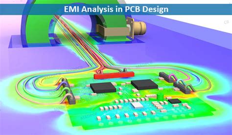
4. EMI/EMC Considerations
Design the PCB to minimize electromagnetic interference (EMI) and ensure electromagnetic compatibility (EMC). Use shielding techniques, such as ground planes and enclosures, to reduce EMI. Follow guidelines for proper grounding and filtering of power supplies.
Power Management Guidelines
Proper power management is essential for maintaining the stability and reliability of the PCB. Here are some guidelines to follow:
1. Power Plane Design
Use dedicated power planes to provide low-impedance power distribution and minimize noise. Separate analog and digital power planes to reduce interference.
2. Decoupling
Place decoupling capacitors close to the power pins of ICs to minimize power supply noise and provide a stable voltage reference. Use a combination of bulk and ceramic capacitors for effective decoupling.
3. Voltage Regulation
Use appropriate voltage regulators to provide stable and clean power to the components. Consider factors such as load current, efficiency, and thermal management when selecting voltage regulators.
4. Power Sequencing
Implement proper power sequencing to ensure that the components receive power in the correct order. This helps prevent damage to sensitive components and ensures proper startup and shutdown behavior.
Thermal Management Guidelines
Managing heat dissipation is critical for ensuring the long-term reliability of the PCB. Here are some guidelines to follow:
1. Component Selection
Select components with appropriate power ratings and thermal characteristics. Consider the maximum operating temperature and the thermal resistance of the components.
2. Thermal Pads and Vias
Use Thermal Pads and vias to provide a low-resistance thermal path from the components to the PCB. This helps dissipate heat and prevents components from overheating.
3. Cooling Mechanisms
Implement appropriate cooling mechanisms, such as heatsinks, fans, and thermal interface materials, to enhance heat dissipation. Consider the airflow and the thermal resistance of the cooling mechanisms.
4. Board Material
Choose a board material with suitable thermal conductivity and Coefficient of Thermal Expansion (CTE) to minimize thermal stresses and improve heat dissipation.
Frequently Asked Questions (FAQ)
-
What is the importance of following PCB design guidelines?
Following PCB design guidelines ensures that the final product is reliable, manufacturable, and meets the desired performance standards. It helps minimize issues related to signal integrity, power management, and thermal management, ultimately leading to a successful electronic product. -
How can I ensure proper signal integrity in my PCB design?
To ensure proper signal integrity, consider the following: - Match the impedance of traces to the source and load impedances.
- Use appropriate termination techniques to minimize reflections.
- Minimize crosstalk by providing adequate spacing and using shielding techniques.
-
Follow guidelines for routing, such as using 45-degree angles and avoiding sharp corners.
-
What are the key considerations for power management in PCB design?
The key considerations for power management include: - Using dedicated power planes for low-impedance power distribution.
- Placing decoupling capacitors close to the power pins of ICs.
- Selecting appropriate voltage regulators based on load current and efficiency.
-
Implementing proper power sequencing to prevent damage to components.
-
How can I manage heat dissipation in my PCB design?
To manage heat dissipation, consider the following: - Select components with appropriate power ratings and thermal characteristics.
- Use thermal pads and vias to provide a low-resistance thermal path.
- Implement cooling mechanisms such as heatsinks and fans.
-
Choose a board material with suitable thermal conductivity and CTE.
-
What are some common mistakes to avoid in PCB design?
Some common mistakes to avoid in PCB design include: - Neglecting to follow design rules and guidelines.
- Improper component placement and orientation.
- Insufficient clearances between components and traces.
- Incorrect trace widths and spacing for the desired impedance and current carrying requirements.
- Neglecting signal integrity considerations, such as impedance matching and crosstalk reduction.
- Inadequate power management and decoupling.
- Overlooking thermal management and heat dissipation requirements.
Conclusion
Designing a reliable and manufacturable PCB requires adherence to a set of well-defined guidelines. By considering key aspects such as component placement, routing, signal integrity, power management, and thermal management, designers can create PCBs that meet the desired performance standards and are cost-effective to produce.
Following the guidelines outlined in this article, such as grouping components, choosing appropriate trace widths and spacing, implementing proper termination and decoupling, and managing heat dissipation, will help ensure the success of your PCB design project.
Remember, PCB design is an iterative process that requires attention to detail and a systematic approach. By keeping the guidelines in mind and leveraging the expertise of experienced designers and manufacturers, you can create PCBs that are reliable, efficient, and meet the demands of your electronic product.


Leave a Reply