What is a PCB Trace Width Calculator?
A PCB trace width calculator is a software tool that helps you calculate the appropriate width for your PCB traces based on various input parameters. These parameters typically include:
- Current: The amount of current that will flow through the trace
- Temperature Rise: The maximum allowable temperature rise of the trace
- Trace Thickness: The thickness of the copper trace
- Trace Length: The length of the trace
- Ambient Temperature: The temperature of the environment in which the PCB will operate
- Copper Weight: The weight of the copper used in the PCB (typically measured in ounces per square foot)
By inputting these parameters into the calculator, it will output the recommended trace width for your specific design.
Why is Trace Width Important?
The width of your PCB traces is crucial for several reasons:
Current Carrying Capacity
The primary purpose of a PCB trace is to carry electrical current from one point to another. The amount of current that a trace can carry is directly related to its width. A wider trace can carry more current than a narrower trace. If you try to push too much current through a trace that is too narrow, it can overheat and potentially fail.
Voltage Drop
As current flows through a trace, there will be a voltage drop across the length of the trace. The amount of voltage drop is dependent on the resistance of the trace, which is directly related to its width. A wider trace will have lower resistance and therefore a lower voltage drop than a narrower trace. If the voltage drop is too high, it can affect the performance of the components connected to the trace.
Temperature Rise
As current flows through a trace, it will generate heat. The amount of heat generated is related to the current and the resistance of the trace. If the trace is too narrow, it will have higher resistance and generate more heat. This can lead to a temperature rise that exceeds the maximum allowable temperature for the PCB material, potentially causing damage or failure.
Signal Integrity
In high-speed digital circuits, the width of the traces can also affect signal integrity. If the traces are too narrow, they can have higher inductance and capacitance, which can cause signal reflections and distortions. This can lead to errors in data transmission and potentially cause the circuit to fail.
How to Use a PCB Trace Width Calculator
Using a PCB trace width calculator is relatively straightforward. Here are the steps you should follow:
-
Gather your design requirements: Before you start using the calculator, you need to know the various parameters that affect trace width, such as the current, temperature rise, trace thickness, etc.
-
Input your design parameters: Once you have your design requirements, input them into the calculator. Make sure to double-check your values to ensure accuracy.
-
Select your units: Most calculators will allow you to select the units for your input parameters, such as amps for current, degrees Celsius for temperature, and millimeters for trace thickness. Make sure to select the appropriate units for your design.
-
Choose your trace material: The calculator will typically have a dropdown menu for selecting the trace material, such as copper or aluminum. Choose the material that matches your design.
-
Calculate your trace width: Once you have input all your parameters and selected your units and material, click the calculate button. The calculator will output the recommended trace width for your design.
-
Verify your results: It’s always a good idea to verify your results by comparing them to industry standards or by running simulations. This will help ensure that your traces are properly sized for your specific application.
Here’s an example of how to use a PCB trace width calculator:
Let’s say you are designing a PCB for a power supply that will carry a maximum current of 5 amps. The trace will be 2 ounces of copper, have a length of 50 mm, and operate in an ambient temperature of 25°C. You want to limit the temperature rise of the trace to 10°C.
Using a trace width calculator, you would input the following parameters:
– Current: 5 A
– Temperature Rise: 10°C
– Trace Thickness: 2 oz
– Trace Length: 50 mm
– Ambient Temperature: 25°C
After inputting these parameters, the calculator would output a recommended trace width of approximately 2.5 mm.

Factors That Affect Trace Width
Several factors can affect the recommended trace width for your PCB design. Understanding these factors can help you make more informed decisions when using a trace width calculator.
Current
The amount of current flowing through your traces is one of the most significant factors affecting trace width. Higher currents require wider traces to prevent overheating and ensure reliable operation. When using a trace width calculator, it’s essential to input the maximum expected current for your design to ensure that your traces are adequately sized.
Temperature Rise
The maximum allowable temperature rise of your traces is another crucial factor to consider. The temperature rise is the difference between the ambient temperature and the maximum temperature that the trace can reach without causing damage. Most PCB materials have a maximum operating temperature of around 125°C, so it’s essential to keep your temperature rise well below this level to ensure long-term reliability.
Trace Thickness
The thickness of your copper traces can also affect the recommended trace width. Thicker traces can carry more current than thinner traces, so if you are using a thicker copper weight, you may be able to use narrower traces. However, thicker traces can also be more expensive and may require more advanced manufacturing techniques.
Trace Length
The length of your traces can also affect the recommended trace width. Longer traces have higher resistance than shorter traces, which can lead to higher voltage drops and temperature rises. When using a trace width calculator, it’s important to input the longest expected trace length to ensure that your traces are adequately sized.
Ambient Temperature
The ambient temperature in which your PCB will operate can also affect the recommended trace width. Higher ambient temperatures will require wider traces to prevent overheating, while lower ambient temperatures may allow for narrower traces. When using a trace width calculator, it’s important to input the expected ambient temperature range for your design.
Copper Weight
The weight of the copper used in your PCB can also affect the recommended trace width. Copper weight is typically measured in ounces per square foot, with common weights being 0.5 oz, 1 oz, and 2 oz. Heavier copper weights can carry more current than lighter weights, but they can also be more expensive and may require more advanced manufacturing techniques.
PCB Trace Width Calculator Tools
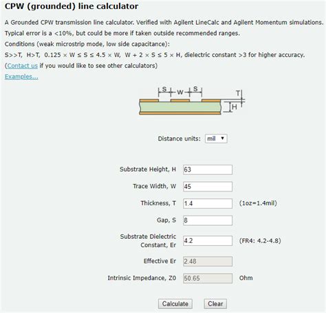
There are many PCB trace width calculator tools available online, both free and paid. Here are a few popular options:
1. 4PCB.com Trace Width Calculator
4PCB.com offers a free trace width calculator that allows you to input your design parameters and get a recommended trace width. The calculator includes options for selecting your copper weight, trace thickness, and ambient temperature.
Link: 4PCB.com Trace Width Calculator
2. Saturn PCB Toolkit
The Saturn PCB Toolkit is a paid software package that includes a trace width calculator along with many other PCB design tools. The trace width calculator allows you to input your design parameters and get a recommended trace width, as well as calculate voltage drops and power dissipation.
Link: Saturn PCB Toolkit
3. EEWeb Trace Width Calculator
EEWeb offers a free online trace width calculator that allows you to input your design parameters and get a recommended trace width. The calculator includes options for selecting your copper weight, trace thickness, and maximum allowable temperature rise.
Link: EEWeb Trace Width Calculator
Best Practices for Using a PCB Trace Width Calculator
While a PCB trace width calculator can be a valuable tool for designing your PCB traces, it’s important to use it correctly to ensure the best results. Here are some best practices to keep in mind:
1. Understand Your Design Requirements
Before using a trace width calculator, it’s essential to have a clear understanding of your design requirements. This includes knowing the maximum expected current, ambient temperature range, and any other relevant parameters. Having accurate input data will help ensure that the calculator provides reliable results.
2. Use Conservative Estimates
When inputting your design parameters into the calculator, it’s always better to use conservative estimates. For example, if you expect your maximum current to be around 3 amps, it’s better to input 4 amps into the calculator to provide some margin for error. Similarly, if you expect your ambient temperature range to be between 20°C and 30°C, it’s better to input 35°C into the calculator to account for any potential temperature spikes.
3. Verify Your Results
While a trace width calculator can provide a good starting point for your trace widths, it’s always a good idea to verify your results through simulation or prototyping. This will help ensure that your traces are properly sized for your specific application and can handle the expected current and temperature ranges.
4. Consider Manufacturing Constraints
When using a trace width calculator, it’s important to keep in mind any manufacturing constraints that may affect your design. For example, if your PCB manufacturer has a minimum trace width of 0.2 mm, you’ll need to ensure that your calculated trace widths are above this minimum. Similarly, if you are using a thicker copper weight, you may need to adjust your trace widths to account for any potential manufacturing difficulties.
5. Document Your Calculations
Finally, it’s important to document your trace width calculations and any assumptions you made during the design process. This will help ensure that your design is reproducible and can be easily modified if necessary. It will also provide a record of your design decisions in case any issues arise during manufacturing or testing.
PCB Trace Width Calculator FAQ
1. What is the difference between internal and external traces?
Internal traces are traces that are located on the inner layers of a multi-layer PCB, while external traces are located on the outer layers. External traces typically have better heat dissipation than internal traces, so they may be able to handle higher currents without overheating. However, internal traces are often used for signal routing and may have tighter spacing requirements.
2. Can I use a trace width calculator for high-frequency signals?
While a trace width calculator can provide a good starting point for high-frequency signal traces, it may not take into account all of the relevant factors such as impedance matching and signal reflection. For high-frequency designs, it’s often necessary to use more advanced simulation tools and follow specific design guidelines to ensure proper signal integrity.
3. What happens if I use traces that are too narrow?
If you use traces that are too narrow for your expected current and temperature range, you risk overheating and damaging your PCB. This can lead to reduced reliability and potentially catastrophic failures. It’s always better to err on the side of caution and use slightly wider traces than necessary rather than risk using traces that are too narrow.
4. Can I use a trace width calculator for flexible PCBs?
Yes, you can use a trace width calculator for flexible PCBs, but you may need to adjust your design parameters to account for the unique properties of flexible materials. For example, flexible PCBs may have lower maximum operating temperatures than rigid PCBs, so you may need to use wider traces to prevent overheating. Additionally, flexible PCBs may have different copper weights and thicknesses than rigid PCBs, so you’ll need to ensure that you are using the correct values in your calculations.
5. How do I account for vias in my trace width calculations?
Vias can have a significant impact on the current carrying capacity and thermal performance of your traces, so it’s important to account for them in your calculations. One approach is to treat the via as a short segment of trace with a different width and thickness than the main trace. You can then calculate the equivalent resistance and temperature rise of the via and add it to your overall trace calculations. Alternatively, some trace width calculators may have built-in options for accounting for vias in your design.
Conclusion
Designing PCBs with the proper trace widths is essential for ensuring the reliability and performance of your electronic devices. Using a PCB trace width calculator can help you quickly and easily determine the appropriate widths for your traces based on your specific design requirements. By following best practices and verifying your results through simulation and prototyping, you can create designs that are optimized for your application and manufacturing processes. With the right tools and knowledge, you can create PCBs that are both reliable and cost-effective, helping to bring your electronic designs to life.


Leave a Reply