What is PCB trace width?
PCB trace width refers to the width of the copper traces that interconnect various components on a printed circuit board. These traces act as the electrical pathways for signals and power to flow between components. The width of these traces plays a crucial role in determining the electrical characteristics, current-carrying capacity, and overall performance of the PCB.
Why is PCB Trace Width Important?
Signal Integrity
One of the primary reasons why PCB trace width is important is its impact on signal integrity. As digital systems continue to operate at higher frequencies and faster data rates, the design of PCB traces becomes increasingly critical to maintain signal quality and minimize signal degradation.
Impedance Matching
Trace width, along with other factors such as dielectric thickness and copper thickness, determines the characteristic impedance of a trace. Proper impedance matching is essential to prevent signal reflections, which can lead to signal distortion, ringing, and other signal integrity issues. By carefully selecting the appropriate trace width, designers can ensure that the trace impedance matches the impedance of the source and load, minimizing signal reflections and improving signal quality.
| Impedance (Ω) | Trace Width (mil) | Dielectric Thickness (mil) | Copper Thickness (oz) |
|---|---|---|---|
| 50 | 20 | 4.7 | 1 |
| 75 | 12 | 4.7 | 1 |
| 100 | 8 | 4.7 | 1 |
Table 1: Example trace width values for different impedance requirements
Crosstalk
Trace width also plays a role in minimizing crosstalk between adjacent traces. Crosstalk occurs when a signal on one trace induces unwanted coupling onto a nearby trace, leading to signal distortion and potentially causing functional issues. By increasing the spacing between traces or using wider traces, designers can reduce the coupling capacitance and minimize crosstalk.
| Trace Spacing (mil) | Crosstalk (dB) |
|---|---|
| 5 | -20 |
| 10 | -30 |
| 20 | -40 |
Table 2: Example crosstalk values for different trace spacings
Power Delivery
Another critical aspect of PCB design where trace width comes into play is power delivery. The width of power and ground traces directly affects the current-carrying capacity and voltage drop across the traces.
Current-Carrying Capacity
The current-carrying capacity of a trace is determined by its cross-sectional area, which is a function of the trace width and copper thickness. Wider traces can carry more current without excessive heating, which is essential for power delivery to high-current components such as processors, FPGAs, and power regulators. Insufficient trace width can lead to excessive voltage drop, power dissipation, and potential reliability issues.
| Trace Width (mil) | Copper Thickness (oz) | Current-Carrying Capacity (A) |
|---|---|---|
| 10 | 1 | 1.0 |
| 20 | 1 | 2.0 |
| 50 | 2 | 7.5 |
Table 3: Example current-carrying capacity values for different trace widths and copper thicknesses
Voltage Drop
Voltage drop is another important consideration in power delivery. As current flows through a trace, there is a voltage drop due to the trace’s resistance. This voltage drop can be minimized by using wider traces, which have lower resistance. Excessive voltage drop can cause components to receive insufficient voltage, leading to performance issues or even component failure.
| Trace Length (in) | Trace Width (mil) | Voltage Drop (mV) |
|---|---|---|
| 2 | 10 | 50 |
| 2 | 20 | 25 |
| 2 | 50 | 10 |
Table 4: Example voltage drop values for different trace lengths and widths
Thermal Management
PCB trace width also plays a role in thermal management. As current flows through a trace, it generates heat due to the trace’s resistance. Wider traces have lower resistance and can dissipate heat more effectively, reducing the temperature rise in the PCB. Proper thermal management is crucial to ensure the long-term reliability and performance of the PCB and its components.
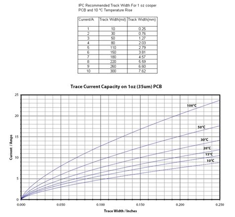
Temperature Rise
The temperature rise in a trace is a function of the current, trace resistance, and the ability of the PCB to dissipate heat. Wider traces have lower resistance and can dissipate heat more efficiently, resulting in lower temperature rise. Designers must carefully consider the expected current levels and ambient temperature conditions to select appropriate trace widths that keep the temperature rise within acceptable limits.
| Trace Width (mil) | Current (A) | Temperature Rise (°C) |
|---|---|---|
| 10 | 1 | 20 |
| 20 | 1 | 10 |
| 50 | 1 | 4 |
Table 5: Example temperature rise values for different trace widths and currents
Manufacturability
Finally, PCB trace width has implications for the manufacturability of the PCB. Trace width and spacing must adhere to the design rules and capabilities of the PCB fabrication process. Overly narrow traces or inadequate spacing can lead to manufacturing issues such as open circuits, short circuits, or poor yields.
Design for Manufacturing (DFM)
Designers must follow the design for manufacturing (DFM) guidelines provided by the PCB manufacturer to ensure the manufacturability of their designs. These guidelines specify the minimum trace width and spacing requirements for different copper weights and PCB classes. Adhering to these guidelines helps to minimize manufacturing defects and improves the overall quality and reliability of the PCB.
| PCB Class | Minimum Trace Width (mil) | Minimum Spacing (mil) |
|---|---|---|
| Class 1 | 10 | 10 |
| Class 2 | 8 | 8 |
| Class 3 | 6 | 6 |
Table 6: Example DFM guidelines for different PCB classes

FAQ
-
What is the recommended trace width for a given current?
The recommended trace width depends on several factors, including the current level, copper thickness, and acceptable temperature rise. Designers can use tools such as trace width calculators or refer to IPC-2152 standards to determine the appropriate trace width for their specific requirements. -
How does trace width affect signal integrity?
Trace width affects signal integrity in several ways. It determines the characteristic impedance of the trace, which is important for impedance matching and minimizing signal reflections. Wider traces also help to reduce crosstalk between adjacent traces by reducing the coupling capacitance. -
Can I use the same trace width for all signals in my design?
No, it is not recommended to use the same trace width for all signals. Different signals have different requirements for impedance, current-carrying capacity, and noise immunity. Designers should carefully consider the specific requirements of each signal and select appropriate trace widths accordingly. -
What happens if the trace width is too narrow?
If the trace width is too narrow, it can lead to various issues such as excessive voltage drop, increased power dissipation, and higher temperature rise. Narrow traces may also violate manufacturing constraints, leading to open circuits or poor yields. It is important to adhere to the minimum trace width requirements specified by the PCB manufacturer. -
How can I balance trace width and routing density?
Balancing trace width and routing density is a common challenge in PCB design. Designers can use techniques such as necking down traces in non-critical areas, using via-in-pad design, or employing high-density interconnect (HDI) techniques to maximize routing density while maintaining appropriate trace widths for signal integrity and power delivery.

Conclusion
PCB trace width is a critical factor in PCB design that directly impacts signal integrity, power delivery, thermal management, and manufacturability. Designers must carefully consider the specific requirements of their design and select appropriate trace widths to ensure optimal performance, reliability, and manufacturability. By understanding the importance of PCB trace width and following best design practices, designers can create high-quality PCBs that meet the demands of today’s complex electronic systems.


Leave a Reply