Introduction to Tenting Vias
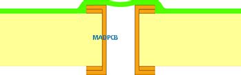
Tenting vias is an important process in the fabrication of printed circuit boards (PCBs). Vias are small holes drilled through a PCB to allow electrical connections between different layers of the board. Tenting refers to covering one or both sides of the via hole with solder mask material. This “tents” over the hole rather than filling it.
Tenting vias serves several key purposes in PCB manufacturing:
- Prevents solder from flowing into via holes during assembly
- Provides a flat, level surface for components and solder joints
- Protects vias from contamination or damage
- Insulates vias to prevent short circuits between layers
- Improves reliability and longevity of the PCB
Without via tenting, the holes can cause issues like uneven surfaces, solder wicking, and shorts that compromise the integrity and functionality of the circuit board. Tenting is especially important for smaller vias and high density designs.
Via Tenting Methods
There are two main methods used for tenting vias in PCB fabrication:
1. Dry Film Solder Mask Tenting
This is the most common method. The via holes are drilled in the bare board. Then a photo-imageable solder mask is applied over the entire surface of the PCB. The solder mask is exposed to UV light through a photo film, which hardens the mask. The unexposed areas are then removed, leaving solder mask covering the via holes.
Advantages of dry film solder mask tenting include:
- Provides complete and uniform coverage
- Works well for small via sizes
- Suitable for both single and double-sided tenting
- Cost-effective for volume production
2. Liquid Photo Imageable (LPI) Solder Mask Tenting
With LPI tenting, a liquid photopolymer solder mask is applied to the PCB surface by screen printing or spraying. It is then exposed to UV light to cure and harden the mask. The LPI process allows for selective tenting of vias.
Advantages of LPI solder mask tenting include:
- Enables tenting of selected vias only
- Provides good coverage for large via holes
- Higher resolution than dry film solder masks
- Faster processing time
The choice between dry film and LPI solder mask tenting depends on factors like via size, design requirements, production volume, and cost considerations.

Design Considerations for Via Tenting
To ensure effective via tenting, several design guidelines should be followed:
-
Via Size: The via drill hole size should be as small as possible while still allowing proper plating and reliable connections. Smaller vias are easier to tent. A typical tented via hole size is 0.2-0.3mm.
-
Pad Size: The via pad (annular ring) should be sized appropriately to provide sufficient area for the solder mask to adhere around the hole. A minimum pad diameter of 0.15mm larger than the drill hole is recommended.
-
Spacing: Adequate space should be maintained between vias and other features like traces, components, and plane areas to prevent tenting issues. A clearance of at least 0.15mm is suggested.
-
Solder Mask Thickness: The solder mask must be applied thick enough over the vias to prevent breakage or solder intrusion. A minimum thickness of 0.01mm over the peak of the via is needed.
-
Via Placement: Vias should be placed thoughtfully in the PCB layout. Avoid locating them under components or connectors. Distribute them evenly to minimize stress and improve manufacturability.
Following these guidelines helps optimize the via tenting process and minimize defects or failures in the finished PCB.

Advantages of Tenting Vias
Tenting vias offers several benefits in PCB manufacturing:
-
Solder Joint Reliability: Tenting prevents solder from wicking into the via holes during reflow soldering. This promotes proper solder joint formation and enhances connection reliability.
-
Surface Flatness: Covering the vias with solder mask provides a flat, level surface for mounting components. This improves placement accuracy and reduces assembly defects.
-
Insulation and Protection: The solder mask tent insulates the vias to prevent short circuits between different layers. It also protects the vias from damage or contamination during handling and use.
-
Smaller Footprint: Via tenting enables the use of smaller via sizes and pad diameters compared to other methods like filling or plugging. This allows for higher density designs and more compact PCB layouts.
-
Cost-Effectiveness: Tenting is generally more economical than filling vias, especially for high volume production. It eliminates the need for additional filling materials and processes.
-
Design Flexibility: Via tenting can be selectively applied to different vias based on design requirements. Both sides of the PCB can be tented for maximum protection.
These advantages make via tenting an attractive option for many PCB applications, particularly those requiring high reliability, small sizes, and cost-efficiency.

Challenges and Limitations
While via tenting is widely used, it does have some potential challenges and limitations:
-
Hole Size Limitations: Tenting very small vias (under 0.2mm) can be difficult, as the solder mask may not adequately cover the hole. Conversely, large vias (over 0.5mm) may have tenting issues due to the greater surface area.
-
Solder Mask Adhesion: If the solder mask does not adhere properly around the via, it can lead to tenting defects like cracks, bubbles, or breakages. This is more likely to occur with higher aspect ratio vias.
-
Thermal Stress: During reflow soldering, the PCB undergoes thermal expansion and contraction. If the solder mask tent is not strong enough, it can crack or break due to the stresses.
-
Impedance Control: For high-frequency PCBs, tenting vias can affect the controlled impedance of the traces. The dielectric constant of the solder mask material must be accounted for in the impedance calculations.
-
Inspection Challenges: Tented vias can be difficult to inspect visually, as the solder mask obscures the hole. Automated optical inspection (AOI) or X-ray inspection may be needed to verify proper tenting.
Despite these challenges, via tenting remains a preferred method for many PCB designers and manufacturers due to its benefits and versatility. Proper design, material selection, and process control can minimize the limitations.
Via Tenting vs. Other Methods
In addition to tenting, there are other methods for dealing with vias in PCBs:
Via Filling
Via filling involves plugging the via holes with a conductive or non-conductive material, typically epoxy or paste. Filled vias provide a completely flat surface and eliminate the need for tenting.
Advantages of via filling:
– Creates a planar surface for component placement
– Provides structural reinforcement to the PCB
– Enables stacking of vias in multilayer designs
– Allows for higher aspect ratio vias
Disadvantages of via filling:
– More expensive and time-consuming than tenting
– Requires additional materials and equipment
– Can be difficult to achieve complete, void-free filling
– May impact electrical performance of the via
Via Plugging
Via plugging is similar to filling, but uses a pre-formed pin or plug to fill the via hole instead of a liquid material. The plugs are typically made of metal or plastic.
Advantages of via plugging:
– Provides a flat surface finish
– Offers good mechanical strength and support
– Suitable for high aspect ratio vias
– Enables efficient assembly processes
Disadvantages of via plugging:
– Higher cost compared to tenting
– Requires precise alignment of plugs with via holes
– May cause stress or damage to the PCB during plugging
– Can affect signal integrity in high-frequency designs
Via Capping
Via capping is a specialized process where a conductive cap is plated or bonded over the top of a filled via. This creates a completely smooth, planar surface for fine-pitch components.
Advantages of via capping:
– Eliminates surface disruptions for optimal component placement
– Provides excellent durability and reliability
– Enables very high-density designs
– Suitable for advanced packaging applications
Disadvantages of via capping:
– Most complex and expensive via protection method
– Requires specialized equipment and processes
– Limited to use with filled vias only
– May impact electrical characteristics of the via
Compared to these alternatives, via tenting offers a simpler, more cost-effective solution for many PCB designs. However, the choice ultimately depends on the specific requirements and constraints of the application.
Tenting Vias for Different Applications
Via tenting is used across a wide range of PCB applications, from simple single-layer boards to complex multilayer designs. Some common applications include:
-
Consumer Electronics: Tenting is widely used in PCBs for consumer devices like smartphones, laptops, gaming systems, and wearables. It helps achieve high-density layouts and reliable performance in compact form factors.
-
Automotive Electronics: Automotive PCBs require robust protection against harsh environmental conditions. Tenting vias helps prevent contamination and failure in applications like engine control units, infotainment systems, and sensors.
-
Medical Devices: Medical PCBs demand high reliability and long lifetimes. Via tenting provides insulation and protection for critical applications like implantable devices, diagnostic equipment, and monitoring systems.
-
Aerospace and Defense: PCBs for aerospace and military use must withstand extreme temperatures, vibrations, and shock. Tenting vias offers mechanical strength and durability for applications like avionics, radar systems, and communication equipment.
-
Industrial Controls: Industrial PCBs are exposed to dust, moisture, and chemicals. Via tenting helps shield the vias from contaminants in applications like factory automation, process control systems, and power electronics.
-
IoT Devices: Internet of Things (IoT) PCBs often have very small sizes and high component densities. Tenting enables the use of micro vias and fine-pitch layouts for applications like sensors, wireless modules, and wearable devices.
The table below summarizes some key considerations for via tenting in different applications:
| Application | Via Size | Solder Mask | Design Priorities |
|---|---|---|---|
| Consumer Electronics | Small (0.2-0.3mm) | Dry film or LPI | High density, reliability |
| Automotive Electronics | Medium (0.3-0.5mm) | Dry film | Durability, protection |
| Medical Devices | Small to medium | Dry film | Reliability, longevity |
| Aerospace/Defense | Medium to large (0.4-0.8mm) | Dry film | Mechanical strength, thermal stability |
| Industrial Controls | Medium | Dry film or LPI | Contamination resistance |
| IoT Devices | Very small (0.1-0.2mm) | Dry film or LPI | Micro vias, fine pitch |
Of course, the specific via tenting requirements will vary depending on the detailed specifications and constraints of each PCB design.
Frequently Asked Questions (FAQ)
- What is the difference between via tenting and via filling?
Via tenting involves covering the via holes with solder mask material, while via filling involves plugging the holes with a conductive or non-conductive material. Tenting leaves the vias open but protected, while filling completely seals the vias.
- Can both sides of a via be tented?
Yes, vias can be tented on one side (single-sided tenting) or both sides (double-sided tenting) of the PCB, depending on the design requirements. Double-sided tenting provides the most complete protection.
- What is the minimum via size that can be reliably tented?
The minimum via size for tenting depends on the capabilities of the PCB manufacturer and the solder mask material. In general, vias as small as 0.2mm in diameter can be tented with modern processes. However, smaller vias may pose challenges for achieving consistent, defect-free tenting.
- How does via tenting affect the electrical performance of a PCB?
Via tenting can have some impact on the electrical characteristics of the PCB, particularly at high frequencies. The solder mask material has a different dielectric constant than the PCB substrate, which can affect impedance and signal integrity. However, these effects are usually minor and can be accounted for in the design process.
- What are some common defects or failures associated with via tenting?
Some potential issues with via tenting include:
- Incomplete or inconsistent coverage of the via holes
- Cracks, bubbles, or breaches in the solder mask tent
- Solder wicking or intrusion into the via during assembly
- Adhesion failures between the solder mask and PCB surface
- Mechanical damage or stress to the tented vias
Proper design, material selection, and process control can help minimize these defects and ensure reliable via tenting.
Conclusion
Via tenting is a critical process in PCB fabrication that provides protection, insulation, and surface leveling for the drilled holes in the board. By covering the vias with solder mask material, tenting enables higher density designs, improved reliability, and cost-effective manufacturing.
As PCB technology continues to advance, via tenting remains an essential technique for achieving the best possible performance and quality in a wide range of applications. By understanding the principles, methods, and design considerations involved in via tenting, PCB designers and manufacturers can optimize their designs and processes to meet the ever-increasing demands of the electronics industry.
Whether for consumer gadgets, automotive systems, medical devices, or industrial controls, via tenting plays a vital role in ensuring that today’s PCBs can deliver the connectivity, functionality, and durability required for a connected world.


Leave a Reply