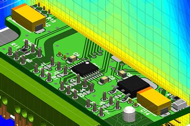
What is PCB cloning?
PCB cloning refers to the process of duplicating an existing printed circuit board (PCB) design. This involves reverse engineering the original PCB to extract the circuit schematic, board layout, and component information, and then using this data to produce an identical copy of the board.
PCB cloning is often used for:
- Replacing obsolete or hard-to-find boards
- Creating backups or spares of critical PCBs
- Analyzing and understanding the design of an existing board
- Modifying or improving upon an existing PCB design
The PCB Cloning Process
The typical steps involved in cloning a PCB are:
-
Obtaining the original PCB: The first step is to acquire the PCB that needs to be cloned. This could be a board from a defunct piece of equipment, a spare part, or a sample obtained for analysis.
-
Reverse engineering: The original PCB is carefully examined and analyzed to determine its structure, components, and connections. This may involve a combination of visual inspection, electrical testing, and specialized tools like microscopes and X-ray machines.
-
Schematic capture: Based on the reverse engineering data, the circuit schematic for the PCB is recreated using Electronic Design Automation (EDA) software. The schematic shows the electrical connections and components that make up the board.
-
PCB layout: Using the schematic as a guide, the physical layout of the PCB is designed in the EDA software. This involves placing the components and routing the traces to create a functional board that matches the original.
-
Fabrication: Once the PCB design is complete, the board is fabricated using standard PCB manufacturing processes. This typically involves printing the circuit pattern onto a copper-clad board, etching away the excess copper, drilling holes, and applying a protective solder mask and silkscreen.
-
Assembly: Finally, the cloned PCB is assembled by soldering on the components according to the original design. The finished board should be functionally identical to the original PCB.
Why Clone PCBs?
There are several reasons why someone might want to clone a PCB:
Obsolescence
One of the most common reasons for cloning PCBs is to replace boards that are no longer being manufactured. As electronic products age, the original PCBs may become obsolete and difficult or impossible to obtain from the original supplier. Cloning allows these old boards to be recreated and used to repair or maintain legacy equipment.
Backup and Spares
Cloning can also be used to create backup copies of critical PCBs. In industries where equipment downtime is costly, having spare boards on hand can help minimize repair times and keep systems running smoothly.
Design Analysis
Cloning a PCB can provide valuable insights into its design and function. By reverse engineering a board, engineers can learn how it works, identify potential weaknesses or areas for improvement, and apply this knowledge to future designs.
Modification and Improvement
Once a PCB has been cloned, it’s possible to modify and improve upon the original design. This could involve updating components, adding new features, or optimizing the layout for better performance or manufacturability. Cloning provides a starting point for these modifications, saving time and effort compared to designing a new board from scratch.

PCB Cloning Techniques
There are several techniques that can be used to clone PCBs, depending on the complexity of the board and the resources available. Some common methods include:
Visual Inspection
For simple PCBs with large, easy-to-identify components, visual inspection may be sufficient to recreate the schematic and layout. This involves carefully examining the board, noting the location and orientation of each component, and tracing the connections between them.
Electrical Testing
More complex boards may require electrical testing to fully understand their function. This can involve using multimeters, oscilloscopes, and other tools to measure voltages, currents, and signals at various points on the board. By systematically testing the board, the cloner can build up a picture of how it works and what each component does.
X-Ray Imaging
For multilayer boards or those with hidden connections, X-ray imaging can be used to see inside the PCB. X-ray machines can create detailed images of the board’s internal structure, showing the location of vias, traces, and other features that would be invisible to the naked eye.
Microscopy
High-magnification microscopes can be used to examine PCBs in fine detail. This can help identify small components, read part numbers, and trace connections between layers.
Schematic Capture Software
Once the structure of the PCB has been determined, schematic capture software is used to create a digital representation of the circuit. This software allows the cloner to draw out the schematic diagram, connecting components together and defining their values and functions.
PCB Layout Software
After the schematic is complete, PCB layout software is used to create the physical design of the board. This involves placing components on the board and routing the traces between them, while ensuring that the design meets all the necessary electrical and manufacturing requirements.

Challenges in PCB Cloning
While PCB cloning is a powerful tool, there are several challenges that can make the process difficult or even impossible in some cases:
Component Identification
One of the biggest challenges in cloning PCBs is identifying all the components on the board. Many components, especially small surface-mount devices, may not have any visible markings or part numbers. In some cases, components may be custom or proprietary, making them difficult to source or replace.
Multilayer Boards
Cloning multilayer PCBs can be much more difficult than single-layer boards. The internal layers of a multilayer board are hidden from view, making it hard to trace connections and determine the board’s structure. X-ray imaging and other advanced techniques may be necessary to fully reverse engineer a multilayer board.
Damaged Boards
If the original PCB is damaged or corroded, it may be difficult or impossible to clone. Missing or destroyed components, broken traces, and other physical damage can make it hard to determine the board’s original design.
Legal Considerations
In some cases, cloning a PCB may be illegal or unethical. Many PCB designs are protected by patents, copyrights, or trade secrets, and cloning them without permission could be considered infringement. It’s important to carefully consider the legal implications before attempting to clone any PCB.

PCB Cloning Tools and Resources
There are many tools and resources available to help with PCB cloning, ranging from simple visual inspection aids to advanced software and hardware. Some of the most useful include:
| Tool | Description |
|---|---|
| Microscope | Used for visual inspection and identification of small components. |
| Multimeter | Used for electrical testing and measuring voltages, currents, and resistances. |
| Oscilloscope | Used for analyzing signals and waveforms on the board. |
| X-Ray Machine | Used for imaging the internal structure of multilayer boards. |
| Schematic Capture SW | Software used to create digital schematics based on reverse engineering data. |
| PCB Layout SW | Software used to design the physical layout of the cloned PCB. |
| PCB Fabrication | Services that can produce physical copies of the cloned PCB based on the digital design files. |
There are also many online communities and forums dedicated to PCB design and reverse engineering, where experts share knowledge and resources related to cloning. Some popular ones include:
- EEVblog Forum
- Hackaday.io
- Dangerous Prototypes Forum
- PCB Heaven Forum
FAQ
Is PCB cloning legal?
The legality of PCB cloning depends on the specific circumstances and the laws of the country where it’s being done. In general, cloning a PCB for personal use or research purposes is usually legal, but cloning and selling a patented or copyrighted design without permission could be considered infringement. It’s important to carefully consider the legal implications before cloning any PCB.
How much does PCB cloning cost?
The cost of cloning a PCB can vary widely depending on the complexity of the board, the tools and techniques used, and whether the cloning is being done in-house or outsourced to a service provider. Simple boards may cost just a few dollars to clone, while complex multilayer boards could cost hundreds or thousands of dollars. In general, the main costs are for the time and expertise required to reverse engineer the board, the software and equipment used for schematic capture and layout, and the fabrication and assembly of the cloned board.
How long does it take to clone a PCB?
The time required to clone a PCB can also vary widely depending on the complexity of the board and the techniques used. Simple boards may be cloned in just a few hours, while complex boards could take days or even weeks to fully reverse engineer and reproduce. In general, the reverse engineering and schematic capture phases are the most time-consuming, while the layout and fabrication phases are relatively quick thanks to modern PCB design software and manufacturing techniques.
Can I clone a PCB myself or do I need to hire a professional?
Whether you can clone a PCB yourself depends on your level of expertise and the tools you have available. Cloning simple boards using visual inspection and manual techniques is within the capabilities of many hobbyists and engineers. However, cloning complex boards with multilayer structures, fine-pitch components, or specialized materials may require advanced equipment and expertise that are beyond the reach of most individuals. In these cases, it may be necessary to hire a professional reverse engineering or PCB design service to clone the board.
What are some alternatives to PCB cloning?
If cloning a PCB is not feasible or desirable, there are a few alternatives that may be appropriate depending on the situation:
-
Redesign: Instead of cloning an existing board, it may be possible to design a new board from scratch that performs the same function. This can be a good option if the original board is obsolete or if improvements are desired.
-
Emulation: In some cases, it may be possible to emulate the function of a PCB using a different hardware platform, such as an FPGA or microcontroller. This can be a good option if the original board is damaged or if a software-based solution is preferred.
-
Substitution: If the original PCB is unavailable but a similar board with compatible functionality is available, it may be possible to substitute the new board in place of the old one. This can be a good option if the original board is obsolete but a newer version or alternative is available.
Ultimately, the best approach will depend on the specific circumstances and requirements of the project.
Conclusion
PCB cloning is a powerful technique for duplicating and analyzing existing printed circuit boards. By reverse engineering a PCB and recreating its schematic and layout, it’s possible to produce functional copies of even the most complex and obscure boards. Cloning can be used to replace obsolete boards, create backups and spares, analyze designs, and even improve upon the original functionality.
However, cloning is not without its challenges. Identifying components, dealing with multilayer structures, and working with damaged boards can all make the cloning process more difficult. It’s also important to carefully consider the legal implications of cloning and to respect the intellectual property rights of the original designers.
Despite these challenges, PCB cloning remains an essential skill for many engineers, technicians, and hobbyists. With the right tools, techniques, and expertise, it’s possible to clone almost any PCB and bring even the most obscure and obsolete boards back to life.


Leave a Reply