The Importance of PCB environmental testing
PCB environmental testing is essential for several reasons:
-
Ensuring product reliability: By subjecting PCBs to various environmental stresses, manufacturers can identify and address potential failure points, ensuring that the final product performs reliably in its intended environment.
-
Meeting industry standards: Many industries have specific environmental testing requirements that PCBs must meet to be certified for use. These standards ensure that products are safe, reliable, and compatible with other components.
-
Reducing warranty claims and recalls: By identifying and addressing issues during the testing phase, manufacturers can minimize the risk of product failures, warranty claims, and costly recalls.
-
Enhancing customer satisfaction: Robust and reliable products that perform well in their intended environment lead to higher customer satisfaction and brand loyalty.
Types of PCB Environmental Tests
There are several types of environmental tests that PCBs undergo during the manufacturing process. Some of the most common tests include:
Temperature Testing
Temperature testing involves exposing PCBs to extreme temperatures to assess their performance and durability. This testing helps identify issues such as component failure, solder joint cracking, and delamination of the PCB layers.
-
High-temperature testing: PCBs are subjected to elevated temperatures (typically up to 150°C) for an extended period to simulate the effects of heat exposure during operation.
-
Low-temperature testing: PCBs are exposed to sub-zero temperatures (as low as -40°C) to evaluate their performance in cold environments.
-
Thermal cycling: PCBs undergo repeated cycles of high and low temperatures to assess their ability to withstand temperature fluctuations and thermal stress.
Humidity Testing
Humidity testing evaluates the PCB’s resistance to moisture and its ability to function in humid environments. High humidity can lead to corrosion, dendrite growth, and reduced insulation resistance.
-
Steady-state humidity testing: PCBs are exposed to a constant high-humidity environment (typically 85% to 95% relative humidity) at an elevated temperature for an extended period.
-
Cyclic humidity testing: PCBs undergo repeated cycles of high and low humidity to simulate real-world conditions and assess their durability.
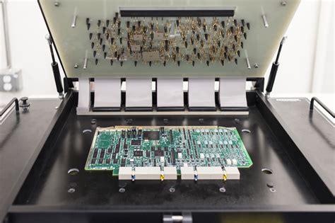
Vibration and Shock Testing
Vibration and shock testing assess the PCB’s ability to withstand mechanical stresses during transportation, handling, and operation.
-
Vibration testing: PCBs are subjected to controlled vibrational forces at various frequencies and amplitudes to simulate real-world conditions, such as those experienced in automotive or aerospace applications.
-
Shock testing: PCBs undergo sudden, high-acceleration impacts to evaluate their resistance to mechanical shocks, such as drops or collisions.
Salt Spray Testing
Salt spray testing evaluates the PCB’s resistance to corrosion in coastal environments or applications where exposure to salt is likely. PCBs are placed in a chamber and exposed to a fine mist of salt solution for an extended period, simulating the effects of long-term exposure to salt-laden air.
Altitude Testing
Altitude testing assesses the PCB’s performance at high altitudes, where reduced air pressure and density can affect component performance and cooling efficiency. This testing is particularly important for applications in the aerospace industry or high-altitude environments.

PCB Environmental Testing Standards
Several international standards govern PCB environmental testing, ensuring consistency and reliability across the industry. Some of the most widely recognized standards include:
-
IPC-9701: A standard for temperature cycling of PCBs, which evaluates the board’s ability to withstand thermal stress.
-
IPC-TM-650: A series of test methods for PCBs, including environmental testing procedures such as temperature, humidity, and salt spray testing.
-
MIL-STD-810: A U.S. Department of Defense standard that outlines environmental testing requirements for military equipment, including PCBs.
-
JEDEC standards: A set of standards developed by the Joint Electron Device Engineering Council (JEDEC) that cover various aspects of PCB testing, including temperature, humidity, and mechanical stress testing.

Environmental Testing in the PCB Manufacturing Process
PCB environmental testing is an integral part of the manufacturing process, typically conducted at several stages to ensure the highest quality and reliability of the final product.
-
Prototype testing: Initial environmental tests are performed on prototype PCBs to identify potential design or material issues early in the development process.
-
Pre-production testing: Before mass production begins, a sample of PCBs undergoes comprehensive environmental testing to validate the design and ensure that the boards meet the required specifications.
-
Production testing: During mass production, periodic environmental tests are conducted on a sample of PCBs to maintain quality control and identify any issues that may arise due to process variations or material changes.
-
Failure analysis: If a PCB fails during environmental testing, a thorough failure analysis is conducted to identify the root cause of the problem and implement corrective actions to prevent future occurrences.

Benefits of PCB Environmental Testing
Investing in comprehensive PCB environmental testing offers several benefits for manufacturers and end-users alike:
-
Improved product quality: By identifying and addressing potential issues early in the development process, manufacturers can produce higher-quality PCBs that perform reliably in their intended environment.
-
Reduced development time and costs: Catching design or material issues early through environmental testing can help reduce development time and costs by avoiding costly redesigns or rework later in the process.
-
Enhanced customer satisfaction: Robust and reliable products that have undergone rigorous environmental testing are more likely to meet or exceed customer expectations, leading to increased satisfaction and brand loyalty.
-
Competitive advantage: Demonstrating a commitment to quality through comprehensive environmental testing can help manufacturers differentiate themselves from competitors and attract customers who prioritize reliability and durability.
Frequently Asked Questions (FAQ)
-
What is the purpose of PCB environmental testing?
PCB environmental testing is conducted to ensure that printed circuit boards can perform reliably and durably in their intended environment, withstanding various stresses such as temperature fluctuations, humidity, vibration, and shock. -
Is PCB environmental testing mandatory?
While not always mandatory, PCB environmental testing is often required to meet industry standards and customer requirements. Many industries, such as automotive, aerospace, and military, have strict environmental testing requirements that PCBs must meet to be certified for use. -
At what stage of the manufacturing process is environmental testing conducted?
Environmental testing is typically conducted at several stages throughout the PCB manufacturing process, including prototype testing, pre-production testing, and production testing. This helps identify and address issues early in the development process and maintain quality control during mass production. -
What are some common environmental tests performed on PCBs?
Common PCB environmental tests include temperature testing (high, low, and thermal cycling), humidity testing (steady-state and cyclic), vibration and shock testing, salt spray testing, and altitude testing. -
How does PCB environmental testing benefit manufacturers and end-users?
PCB environmental testing helps manufacturers improve product quality, reduce development time and costs, enhance customer satisfaction, and gain a competitive advantage. End-users benefit from more reliable and durable products that perform well in their intended environment.
| Test Type | Purpose | Conditions |
|---|---|---|
| Temperature Testing | Evaluate PCB performance and durability under extreme temperatures | High temperature (up to 150°C), low temperature (down to -40°C), thermal cycling |
| Humidity Testing | Assess PCB resistance to moisture and performance in humid environments | Steady-state humidity (85-95% RH), cyclic humidity |
| Vibration and Shock Testing | Determine PCB’s ability to withstand mechanical stresses during transportation, handling, and operation | Controlled vibrational forces at various frequencies and amplitudes, sudden high-acceleration impacts |
| Salt Spray Testing | Evaluate PCB’s resistance to corrosion in coastal environments or applications exposed to salt | Exposure to fine mist of salt solution for extended periods |
| Altitude Testing | Assess PCB performance at high altitudes with reduced air pressure and density | Simulation of high-altitude environments, particularly important for aerospace applications |
In conclusion, PCB environmental testing is a critical process in the manufacturing of electronic devices, ensuring their reliability, durability, and performance under various environmental conditions. By subjecting PCBs to a range of tests, including temperature, humidity, vibration, shock, salt spray, and altitude testing, manufacturers can identify potential issues early in the development process, reduce costs and time to market, and ultimately deliver high-quality products that meet or exceed customer expectations. As the electronics industry continues to evolve and new applications emerge, the importance of comprehensive PCB environmental testing will only continue to grow, driving innovation and improving the overall quality and reliability of electronic devices.


Leave a Reply