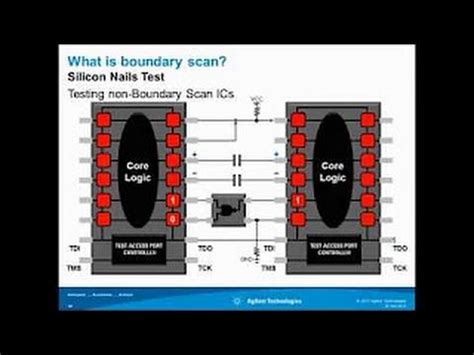
What is Boundary-Scan Testing?
Boundary-scan testing is a method used to test the interconnections between integrated circuits (ICs) on a PCB. It utilizes a special set of test circuits built into the ICs themselves, allowing for the testing of the connections between them without the need for physical access to the pins. The boundary-scan architecture consists of a series of boundary-scan cells, each associated with an IC pin, that can capture and control the state of the pin.
The boundary-scan testing process involves shifting test patterns into the boundary-scan cells, applying the patterns to the PCB interconnections, and then capturing and shifting out the results for analysis. This enables the detection of various faults, such as open circuits, short circuits, and stuck-at faults, which may not be easily detectable through other testing methods.
Benefits of Boundary-Scan Testing
1. Improved Fault Coverage
One of the primary benefits of boundary-scan testing is its ability to provide comprehensive fault coverage. Traditional testing methods, such as in-circuit testing (ICT) or flying probe testing, may struggle to access certain components or test points due to the increasing density and complexity of modern PCBs. Boundary-scan testing overcomes these limitations by utilizing the built-in test circuitry within the ICs themselves.
With boundary-scan testing, it is possible to test the interconnections between ICs, regardless of their physical accessibility. This means that even components with fine-pitch or ball grid array (BGA) packages can be effectively tested. By testing the interconnections at the IC level, boundary-scan testing can detect faults that may otherwise go unnoticed, such as opens, shorts, and stuck-at faults.
2. Reduced Test Development Time
Developing test programs for traditional testing methods can be a time-consuming process. It often requires the creation of custom test fixtures and the development of complex test sequences to cover all the necessary test points. With boundary-scan testing, the test development process is significantly simplified.
Since boundary-scan testing relies on the built-in test circuitry within the ICs, the need for custom test fixtures is eliminated. The test patterns can be generated automatically based on the PCB design data, such as the netlist and the boundary-scan description language (BSDL) files provided by the IC manufacturers. This automation reduces the time and effort required to develop test programs, allowing for faster time-to-market and more efficient testing cycles.
3. Non-Invasive Testing
Another advantage of boundary-scan testing is its non-invasive nature. Traditional testing methods often require physical access to the PCB, which can be challenging in cases where the components are densely packed or have limited access points. Probing the PCB with test probes or fixtures can potentially cause damage to the components or the board itself.
Boundary-scan testing, on the other hand, does not require physical access to the PCB. The test patterns are applied and captured through the boundary-scan cells within the ICs, eliminating the need for probing or direct contact with the components. This non-invasive approach reduces the risk of damage during the testing process and ensures the integrity of the PCB.
4. Reduced Test Costs
Implementing boundary-scan testing can lead to significant cost savings in the long run. Traditional testing methods often require expensive test fixtures and specialized equipment, which can be costly to develop and maintain. Additionally, the time and labor involved in setting up and executing these tests can contribute to higher overall testing costs.
Boundary-scan testing, with its simplified test development process and reduced reliance on custom fixtures, can help minimize these costs. The automated generation of test patterns and the ability to test multiple ICs simultaneously can speed up the testing process, reducing the time and labor required. Furthermore, the non-invasive nature of boundary-scan testing reduces the risk of damage to the PCB, which can save on repair and rework costs.
5. Enhanced Diagnostics and Debugging
Boundary-scan testing provides powerful diagnostic and debugging capabilities. When a fault is detected during the testing process, boundary-scan tools can pinpoint the exact location and nature of the fault. This detailed fault information enables engineers to quickly identify and resolve issues, reducing the time spent on troubleshooting and debugging.
Moreover, boundary-scan testing allows for interactive debugging sessions. Engineers can control and observe the state of individual pins, inject test patterns, and analyze the response in real-time. This interactive debugging capability facilitates the isolation and resolution of complex faults that may be difficult to diagnose through other means.
6. Compatibility with Other Testing Methods
Boundary-scan testing is not a standalone solution but can be integrated with other testing methods to create a comprehensive testing strategy. It complements traditional testing techniques, such as in-circuit testing and functional testing, by providing additional fault coverage and diagnostic capabilities.
For example, boundary-scan testing can be used to test the interconnections between ICs, while in-circuit testing can verify the proper functioning of individual components. By combining different testing methods, manufacturers can ensure thorough coverage and catch a wider range of faults, resulting in higher quality and reliability of the PCBs.

Implementing Boundary-Scan Testing
To implement boundary-scan testing, certain requirements need to be met. First and foremost, the ICs on the PCB must be boundary-scan compliant. This means that they must have the necessary boundary-scan architecture and support the IEEE 1149.1 standard, which defines the boundary-scan interface and protocol.
Additionally, the PCB design must incorporate the necessary boundary-scan infrastructure, such as the Test Access Port (TAP) and the boundary-scan chain. The TAP serves as the interface between the boundary-scan circuitry and the external test equipment, while the boundary-scan chain connects the boundary-scan cells of the ICs in a serial fashion.
To facilitate the implementation of boundary-scan testing, various tools and solutions are available in the market. These tools often provide a user-friendly interface for generating test patterns, executing tests, and analyzing results. They may also offer integration with other design and testing tools, such as PCB design software and in-circuit testers, to streamline the overall testing process.

Frequently Asked Questions (FAQ)
1. Is boundary-scan testing suitable for all types of PCBs?
Boundary-scan testing is particularly beneficial for PCBs with high component density, fine-pitch packages, and limited physical access. However, it requires the ICs on the PCB to be boundary-scan compliant. If the PCB contains non-compliant ICs, boundary-scan testing may have limited coverage, and additional testing methods may be necessary.
2. Can boundary-scan testing replace traditional testing methods?
Boundary-scan testing is not a replacement for traditional testing methods but rather a complementary technique. While it excels in testing interconnections between ICs, it may not cover all aspects of PCB functionality. A comprehensive testing strategy often involves a combination of boundary-scan testing, in-circuit testing, functional testing, and other methods to ensure thorough fault coverage.
3. How does boundary-scan testing handle analog components?
Boundary-scan testing primarily focuses on digital components and their interconnections. Analog components, such as resistors, capacitors, and inductors, cannot be directly tested using boundary-scan techniques. However, boundary-scan testing can still be used to test the digital portions of mixed-signal ICs that contain both analog and digital circuitry.
4. What are the limitations of boundary-scan testing?
One limitation of boundary-scan testing is that it relies on the availability of boundary-scan compliant ICs. If the PCB contains non-compliant ICs, the fault coverage may be reduced. Additionally, boundary-scan testing focuses on the interconnections between ICs and may not detect faults within the ICs themselves. It is important to use boundary-scan testing in conjunction with other testing methods to ensure comprehensive fault coverage.
5. How does boundary-scan testing handle high-speed interfaces?
Boundary-scan testing can be applied to high-speed interfaces, such as DDR memory or PCI Express, with certain considerations. The boundary-scan cells need to be designed to handle the high-speed signals without introducing signal integrity issues. Special boundary-scan techniques, such as AC coupling or differential signaling, may be employed to accommodate high-speed interfaces. It is important to consult the IC manufacturer’s guidelines and use appropriate boundary-scan tools that support high-speed testing.

Conclusion
Boundary-scan testing is a powerful technique that offers numerous benefits for PCB assembly. By providing comprehensive fault coverage, reducing test development time, enabling non-invasive testing, reducing test costs, enhancing diagnostics and debugging, and complementing other testing methods, boundary-scan testing has become an essential tool in ensuring the quality and reliability of PCBs.
As PCBs continue to evolve in complexity and density, boundary-scan testing will play an increasingly important role in the electronics manufacturing industry. By embracing boundary-scan testing and integrating it into their testing strategies, manufacturers can streamline their testing processes, improve product quality, and reduce time-to-market.
However, it is important to recognize that boundary-scan testing is not a one-size-fits-all solution. It should be used in conjunction with other testing methods to create a comprehensive testing approach tailored to the specific requirements of each PCB. By leveraging the strengths of boundary-scan testing and combining it with traditional testing techniques, manufacturers can achieve the highest levels of quality and reliability in their PCB assemblies.
As technology advances and new challenges arise, the importance of effective testing methods like boundary-scan testing will only continue to grow. By staying informed about the latest developments in boundary-scan testing and investing in the necessary tools and expertise, manufacturers can position themselves for success in the ever-evolving world of electronics manufacturing.
| Comparison Criteria | Boundary-Scan Testing | Traditional Testing Methods |
|---|---|---|
| Fault Coverage | High | Limited |
| Test Development Time | Reduced | Longer |
| Invasiveness | Non-invasive | Potentially invasive |
| Test Costs | Lower | Higher |
| Diagnostics and Debugging | Enhanced | Limited |
| Compatibility | Complementary | Standalone |
In summary, boundary-scan testing offers a range of benefits that can significantly improve the efficiency, effectiveness, and cost-effectiveness of PCB testing. By leveraging the power of boundary-scan testing, manufacturers can ensure the highest levels of quality and reliability in their PCB assemblies, ultimately leading to greater customer satisfaction and business success.


Leave a Reply