Introduction to PCB Inspection
PCB (Printed Circuit Board) inspection is a critical step in the PCB assembly process that ensures the quality and reliability of the final product. It involves examining the PCB for any defects or anomalies that may affect its functionality or performance. PCB inspection plays a vital role in identifying and correcting issues before the PCB is assembled into a finished product, reducing the risk of failures and improving overall product quality.
The Importance of PCB Inspection
PCB inspection is essential for several reasons:
-
Quality Assurance: PCB inspection helps to identify any defects or issues that may compromise the quality of the final product. By detecting these problems early in the assembly process, manufacturers can take corrective action and prevent defective PCBs from being used in finished products.
-
Cost Savings: Identifying and correcting PCB defects early in the assembly process can save manufacturers significant costs associated with rework, repairs, and product returns. By catching issues before the PCB is assembled into a finished product, manufacturers can avoid the expense of replacing defective components or entire products.
-
Reliability: PCB inspection helps to ensure that the final product is reliable and performs as intended. By identifying and correcting defects, manufacturers can reduce the risk of product failures and improve overall product reliability.
-
Compliance: PCB inspection is often required to meet industry standards and regulations, such as IPC (Association Connecting Electronics Industries) standards. By adhering to these standards, manufacturers can ensure that their products meet the necessary quality and reliability requirements.
Types of PCB Inspection
There are several types of PCB inspection methods used in the assembly process, each with its own advantages and limitations. Some of the most common PCB inspection methods include:
1. Visual Inspection
Visual inspection is the most basic form of PCB inspection and involves examining the PCB with the naked eye or using magnification tools. This method is often used to check for obvious defects such as missing components, incorrect component placement, or visible damage to the PCB.
Advantages:
– Low cost
– Quick and easy to perform
– Can identify obvious defects
Limitations:
– Limited to detecting visible defects
– Subjective and dependent on the inspector’s skill and experience
– Not suitable for detecting more subtle or internal defects
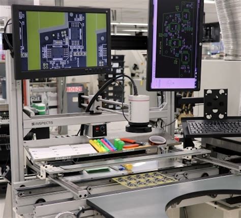
2. Automated Optical Inspection (AOI)
Automated Optical Inspection (AOI) uses specialized cameras and image processing software to automatically inspect PCBs for defects. AOI systems can quickly scan the entire PCB and compare it to a reference image to identify any anomalies or deviations.
Advantages:
– Fast and efficient inspection of large volumes of PCBs
– Objective and consistent results
– Can detect a wide range of defects, including component placement, solder joint quality, and trace integrity
Limitations:
– Higher initial cost compared to manual inspection methods
– Limited to detecting surface-level defects
– May require programming and setup for each specific PCB design
3. X-Ray Inspection
X-ray inspection uses X-ray imaging to examine the internal structure of the PCB, including solder joints and component connections. This method is particularly useful for detecting defects that are not visible on the surface of the PCB.
Advantages:
– Can detect internal defects, such as voids in solder joints or broken connections
– Non-destructive testing method
– Provides detailed images of the PCB’s internal structure
Limitations:
– Higher cost compared to other inspection methods
– Requires specialized equipment and trained operators
– May be slower than other inspection methods
4. In-Circuit Testing (ICT)
In-Circuit Testing (ICT) involves using a specialized test fixture to electrically test the PCB and its components. ICT can detect a wide range of defects, including short circuits, open circuits, and incorrect component values.
Advantages:
– Can detect both visible and non-visible defects
– Provides functional testing of the PCB and its components
– Can be automated for high-volume testing
Limitations:
– Requires the development of a custom test fixture for each PCB design
– May be more time-consuming than other inspection methods
– Limited to testing the electrical functionality of the PCB

PCB Inspection in the Assembly Process
PCB inspection is typically performed at several stages throughout the assembly process to ensure that defects are identified and corrected as early as possible. Some of the key stages where PCB inspection is performed include:
1. Incoming Material Inspection
Before the PCB assembly process begins, the incoming materials, such as PCB bare boards and components, are inspected to ensure that they meet the required specifications and are free from defects. This inspection may include visual inspection, dimensional checks, and electrical testing.
2. Solder Paste Inspection (SPI)
After the solder paste is applied to the PCB, but before components are placed, Solder Paste Inspection (SPI) is performed to ensure that the solder paste is applied correctly and consistently. SPI uses specialized cameras and image processing software to measure the volume, height, and position of the solder paste deposits.
3. Pre-Reflow Inspection
After the components are placed on the PCB, but before the solder reflow process, a pre-reflow inspection is performed to ensure that all components are placed correctly and securely. This inspection may include visual inspection, AOI, or X-ray inspection, depending on the complexity of the PCB and the types of components used.
4. Post-Reflow Inspection
After the solder reflow process is complete, a post-reflow inspection is performed to ensure that the solder joints are formed correctly and that there are no defects such as bridging, insufficient solder, or voids. This inspection may include visual inspection, AOI, X-ray inspection, or a combination of methods.
5. Functional Testing
After the PCB assembly is complete, functional testing is performed to ensure that the PCB operates as intended and meets the required performance specifications. This testing may include In-Circuit Testing (ICT), boundary scan testing, or functional testing using specialized test equipment.

Common PCB Defects and Their Causes
Despite the best efforts of manufacturers to control the PCB assembly process, defects can still occur. Some of the most common PCB defects and their causes include:
1. Solder Bridges
Solder bridges occur when excess solder creates an unintended connection between two or more solder pads or traces. Causes of solder bridges include:
- Excess solder paste application
- Incorrect solder stencil design
- Improper component placement
- Incorrect reflow profile
2. Insufficient Solder
Insufficient solder occurs when there is not enough solder to create a proper connection between the component and the PCB. Causes of insufficient solder include:
- Insufficient solder paste application
- Incorrect solder stencil design
- Poor wetting of the solder pads
- Incorrect reflow profile
3. Component Shifting
Component shifting occurs when components move from their intended position during the solder reflow process. Causes of component shifting include:
- Improper component placement
- Insufficient solder paste application
- Incorrect reflow profile
- Vibration or movement during the reflow process
4. Tombstoning
Tombstoning occurs when a component stands up on one end during the solder reflow process, creating an open circuit. Causes of tombstoning include:
- Uneven heating during the reflow process
- Incorrect component placement
- Insufficient solder paste application
- Incorrect pad design

Best Practices for Effective PCB Inspection
To ensure effective PCB inspection and minimize the risk of defects, manufacturers should follow these best practices:
-
Establish Inspection Standards: Develop and document clear inspection standards and criteria based on industry guidelines, such as IPC standards, and customer requirements.
-
Use Appropriate Inspection Methods: Select the most appropriate inspection methods based on the complexity of the PCB, the types of components used, and the potential defects that may occur.
-
Implement Statistical Process Control (SPC): Use SPC techniques to monitor and control the PCB assembly process, identifying trends and variations that may indicate potential defects or issues.
-
Train Inspection Personnel: Ensure that inspection personnel are properly trained on the inspection standards, methods, and equipment used in the PCB assembly process.
-
Regularly Maintain and Calibrate Inspection Equipment: Regularly maintain and calibrate inspection equipment to ensure accurate and consistent results.
-
Continuously Improve the Inspection Process: Continuously monitor and analyze inspection data to identify areas for improvement and implement corrective actions to prevent future defects.
The Future of PCB Inspection
As PCB technology continues to advance and become more complex, PCB inspection methods must also evolve to keep pace. Some of the emerging trends and technologies in PCB inspection include:
-
3D Automated Optical Inspection (3D AOI): 3D AOI systems use multiple cameras and advanced image processing algorithms to create a three-dimensional model of the PCB, allowing for more accurate and comprehensive defect detection.
-
Artificial Intelligence (AI) and Machine Learning (ML): AI and ML technologies are being integrated into PCB inspection systems to improve defect detection accuracy and reduce false positives. These technologies can learn from past inspection data to continually improve their performance over time.
-
Inline Inspection Systems: Inline inspection systems are integrated directly into the PCB assembly line, allowing for real-time defect detection and correction. This approach can help to reduce the time and cost associated with offline inspection methods.
-
Big Data Analytics: As PCB inspection systems generate increasing amounts of data, big data analytics tools can be used to analyze this data and identify trends, patterns, and insights that can help to improve the PCB assembly process and reduce defects.
Frequently Asked Questions (FAQ)
- What is the difference between AOI and visual inspection?
-
AOI is an automated process that uses cameras and image processing software to detect defects, while visual inspection is a manual process that relies on the human eye and magnification tools to identify defects. AOI is faster, more consistent, and can detect a wider range of defects compared to visual inspection.
-
How often should PCB inspection be performed during the assembly process?
-
PCB inspection should be performed at several key stages throughout the assembly process, including incoming material inspection, solder paste inspection, pre-reflow inspection, post-reflow inspection, and functional testing. The specific frequency and type of inspection will depend on the complexity of the PCB and the potential defects that may occur.
-
What are the most common causes of PCB defects?
-
Some of the most common causes of PCB defects include incorrect solder paste application, improper component placement, incorrect reflow profiles, and poor wetting of solder pads. Other factors such as contamination, moisture, and handling can also contribute to PCB defects.
-
Can all PCB defects be detected through inspection?
-
While PCB inspection methods can detect a wide range of defects, some defects may be difficult or impossible to detect through inspection alone. For example, some internal defects or intermittent issues may only be detectable through functional testing or other specialized testing methods.
-
How can manufacturers ensure the effectiveness of their PCB inspection process?
- To ensure the effectiveness of their PCB inspection process, manufacturers should establish clear inspection standards, use appropriate inspection methods, implement statistical process control, train inspection personnel, regularly maintain and calibrate inspection equipment, and continuously improve the inspection process based on data and feedback.
Conclusion
PCB inspection plays a critical role in ensuring the quality, reliability, and performance of PCB assemblies. By identifying and correcting defects early in the assembly process, manufacturers can reduce costs, improve product quality, and meet industry standards and customer requirements. As PCB technology continues to evolve, so too must PCB inspection methods and technologies to keep pace with the increasing complexity and demands of the industry. By adopting best practices and embracing emerging technologies, manufacturers can stay ahead of the curve and deliver high-quality PCB assemblies that meet the needs of their customers.


Leave a Reply