Introduction to PCB cloning
PCB (Printed Circuit Board) cloning is the process of creating an exact replica of an existing PCB design. This technique is widely used in the electronics industry for various purposes, such as reproducing legacy designs, reverse engineering, and prototyping. PCB cloning involves analyzing the original board, extracting the design information, and using it to manufacture a new, identical PCB.
In this comprehensive article, we will dive deep into the world of PCB cloning, exploring its working principles, advantages, and applications. We will also discuss the tools and techniques used in the cloning process and provide a step-by-step guide to help you understand how to clone a PCB.
Understanding the Basics of PCBs
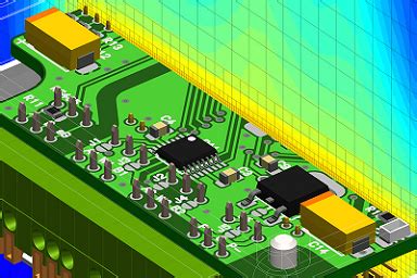
Before we delve into the specifics of PCB cloning, let’s first understand the basics of PCBs. A PCB is a flat, insulating board that supports and connects electronic components using conductive tracks, pads, and other features etched from copper sheets laminated onto a non-conductive substrate. PCBs are used in almost all electronic devices, from simple consumer gadgets to complex industrial equipment.
PCBs come in various types, depending on their structure and the number of layers:
- Single-sided PCBs: These have conductive tracks on only one side of the board.
- Double-sided PCBs: These have conductive tracks on both sides of the board, with the two sides connected through vias (holes).
- Multi-layer PCBs: These have multiple layers of conductive tracks, separated by insulating layers, allowing for more complex designs and higher component density.
| PCB Type | Layers | Complexity | Applications |
|---|---|---|---|
| Single-sided | 1 | Low | Simple consumer electronics |
| Double-sided | 2 | Medium | More advanced devices |
| Multi-layer | 3+ | High | Complex industrial equipment |

Why Clone a PCB?
There are several reasons why you might need to clone a PCB:
-
Reproducing legacy designs: When a company needs to replace or repair an old device for which the original PCB design files are no longer available, PCB cloning can help recreate the design.
-
Reverse engineering: Cloning a PCB can help understand how a device works, allowing for modifications, improvements, or the creation of compatible products.
-
Prototyping: When developing a new product, cloning an existing PCB with similar functionality can save time and resources in the prototyping phase.
-
Educational purposes: PCB cloning can be a valuable learning tool for students and hobbyists interested in understanding electronic circuit design and manufacturing processes.

The PCB Cloning Process
The PCB cloning process typically involves the following steps:
Step 1: Acquiring the Original PCB
The first step in PCB cloning is to obtain the original PCB that you want to clone. This can be an old, damaged, or obsolete board that needs to be replaced or a competitor’s product that you want to analyze or modify.
Step 2: Visual Inspection and Documentation
Before starting the cloning process, thoroughly inspect the original PCB and document its features, such as component placement, connectors, and any visible markings or labels. Take high-resolution photographs of both sides of the board for reference.
Step 3: Schematic Diagram Creation
If the schematic diagram of the original PCB is not available, you’ll need to create one by analyzing the board’s components and their interconnections. This can be done manually or using specialized software tools that can help identify components and trace the circuit paths.
Step 4: PCB Layout Design
Once you have the schematic diagram, you can proceed to design the PCB layout. This involves determining the board size, layer structure, component placement, and routing of the conductive tracks. PCB design software, such as Altium Designer, Eagle, or KiCad, can be used for this purpose.
Step 5: Manufacturing and Assembly
After finalizing the PCB layout, the design files are sent to a PCB manufacturing service provider. They will fabricate the board according to your specifications and, if requested, assemble the components onto the board. The result is a cloned PCB that is functionally identical to the original.

Tools and Techniques for PCB Cloning
Several tools and techniques are used in the PCB cloning process, depending on the complexity of the board and the available resources:
-
Visual inspection tools: These include magnifying glasses, microscopes, and high-resolution cameras that help in examining the original PCB and documenting its features.
-
Schematic capture tools: Software tools like Eagle, KiCad, or Altium Designer can be used to create schematic diagrams based on the analysis of the original PCB.
-
PCB design software: The same software tools used for schematic capture are also used for PCB layout design. These tools provide features like automatic routing, design rule checking, and 3D visualization.
-
PCB scanners: Advanced PCB scanners can automatically analyze the original board and generate design files, significantly reducing the time and effort required for manual tracing and schematic creation.
-
X-ray imaging: For complex multi-layer PCBs, X-ray imaging can be used to visualize the internal layers and trace the interconnections between components.
Advantages of PCB Cloning
PCB cloning offers several advantages, making it a valuable technique in the electronics industry:
-
Cost-effective: Cloning an existing PCB design is often more cost-effective than designing a new board from scratch, especially for small-scale production or prototyping.
-
Time-saving: By leveraging an existing design, PCB cloning can significantly reduce the time required for development and testing.
-
Improved reliability: Cloning a PCB that has already been proven to work can minimize the risk of design errors and ensure the reliability of the cloned board.
-
Customization: PCB cloning allows for modifications and improvements to the original design, enabling customization to suit specific requirements or applications.
Challenges and Considerations in PCB Cloning
While PCB cloning offers numerous benefits, there are also some challenges and considerations to keep in mind:
-
Intellectual property: Cloning a PCB without the owner’s permission may infringe on their intellectual property rights. It’s essential to ensure that you have the necessary permissions or licenses before cloning a PCB.
-
Component availability: If the original PCB uses obsolete or hard-to-find components, sourcing them for the cloned board may be challenging or expensive.
-
Manufacturing limitations: Some complex PCB designs may require specialized manufacturing processes or materials that may not be readily available or cost-effective for small-scale production.
-
Debugging and testing: Even with a successfully cloned PCB, debugging and testing may be necessary to ensure that the board functions as intended and meets the required specifications.
Frequently Asked Questions (FAQ)
-
Q: Is PCB cloning legal?
A: PCB cloning is legal as long as you have the necessary permissions or licenses from the original design owner. Cloning a PCB without permission may infringe on intellectual property rights. -
Q: Can I clone a multi-layer PCB?
A: Yes, multi-layer PCBs can be cloned using advanced techniques like X-ray imaging to trace the internal layers and interconnections. -
Q: How long does it take to clone a PCB?
A: The time required for PCB cloning depends on the complexity of the board and the available resources. Simple boards can be cloned in a few days, while complex designs may take several weeks. -
Q: What is the cost of PCB cloning?
A: The cost of PCB cloning varies depending on factors such as the board complexity, the number of layers, and the manufacturing and assembly requirements. However, cloning is generally more cost-effective than designing a new board from scratch. -
Q: Can I modify the original design when cloning a PCB?
A: Yes, PCB cloning allows for modifications and improvements to the original design to suit specific requirements or applications.
Conclusion
PCB cloning is a powerful technique that enables the reproduction, analysis, and modification of existing PCB designs. By leveraging tools and techniques like visual inspection, schematic capture, and PCB design software, it is possible to create exact replicas of PCBs for various purposes, such as legacy design reproduction, reverse engineering, and prototyping.
While PCB cloning offers numerous advantages, including cost-effectiveness, time-saving, and improved reliability, it is essential to consider the challenges and legal implications involved in the process. By understanding the principles, tools, and techniques of PCB cloning, electronics professionals and hobbyists can harness its potential to create innovative and reliable electronic devices.


Leave a Reply