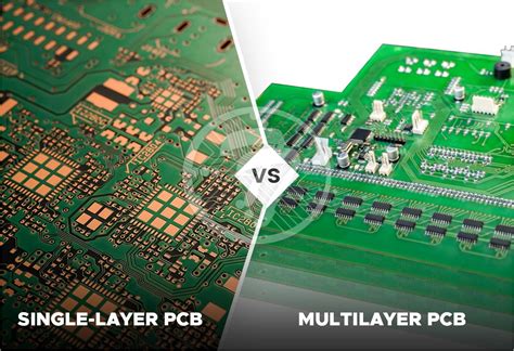
What are Multilayer PCBs?
Multilayer PCBs are printed circuit boards that consist of three or more conductive copper layers separated by insulating material. These layers are interconnected through vias, which are small holes drilled through the board and plated with conductive material. The multiple layers allow for a higher density of components and more complex circuitry compared to single or double-layer boards.
Advantages of Multilayer PCBs
- Increased circuit density
- Improved signal integrity
- Reduced electromagnetic interference (EMI)
- Better heat dissipation
- Smaller form factor

Common Limitations of Multilayer PCBs
Despite their numerous benefits, multilayer PCBs come with their own set of limitations that can impact the design, manufacturing, and performance of the final product.
Signal Integrity Issues
As the number of layers increases, so does the potential for signal integrity issues. These issues can arise from factors such as crosstalk, impedance mismatch, and signal reflections. Crosstalk occurs when signals from one trace interfere with those of another, leading to signal distortion and potential malfunctions. Impedance mismatch happens when there is a difference in the characteristic impedance between the trace and the connected component, causing signal reflections and degrading signal quality.
Solutions for Signal Integrity Issues
- Proper trace routing and spacing
- Use of ground planes and power planes
- Impedance matching techniques
- Implementation of differential signaling
- Application of signal integrity simulation tools
Thermal Management Challenges
Multilayer PCBs can generate significant amounts of heat due to the high density of components and the increased power consumption. If not managed properly, this heat can lead to component failure, reduced performance, and even board warpage. Thermal management becomes more challenging as the number of layers increases, as the heat needs to be dissipated through multiple layers of insulating material.
Solutions for Thermal Management Challenges
- Use of thermal vias and heat sinks
- Proper component placement and spacing
- Selection of materials with high thermal conductivity
- Incorporation of active cooling methods (e.g., fans, heatsinks)
- Thermal simulation and analysis during the design phase
Manufacturing Complexity
The manufacturing process for multilayer PCBs is more complex and time-consuming compared to single or double-layer boards. The increased number of layers requires more precise alignment and registration during the lamination process, as well as additional drilling and plating steps. This complexity can lead to higher manufacturing costs and longer lead times.
Solutions for Manufacturing Complexity
- Use of advanced manufacturing techniques (e.g., Sequential Lamination)
- Implementation of strict quality control measures
- Collaboration with experienced and reliable PCB manufacturers
- Utilization of design for manufacturability (DFM) principles
- Adoption of automated inspection and testing methods
Cost Considerations
Multilayer PCBs are generally more expensive to design and manufacture compared to simpler board configurations. The cost increases with the number of layers, as well as the complexity of the circuit design and the materials used. This can be a significant limitation for projects with tight budgets or high-volume production requirements.
Solutions for Cost Considerations
- Optimization of the layer stackup and circuit design
- Use of cost-effective materials and components
- Consideration of alternative manufacturing methods (e.g., high-density interconnect)
- Negotiation of volume discounts with PCB manufacturers
- Implementation of design for cost (DFC) principles

Overcoming Multilayer PCB Limitations through Advanced Technologies
In recent years, several advanced technologies have emerged that can help overcome the limitations of multilayer PCBs and enable the design and manufacture of even more complex and high-performance boards.
High-Density Interconnect (HDI) Technology
HDI technology involves the use of microvias and fine-pitch traces to achieve higher circuit densities and improved signal integrity. Microvias are small, laser-drilled holes that connect the outer layers of the PCB to the inner layers, allowing for more efficient use of space and reducing the need for traditional through-hole vias. Fine-pitch traces are narrower and more closely spaced than standard traces, enabling tighter component placement and shorter signal paths.
| HDI Characteristic | Benefit |
|---|---|
| Microvias | Higher circuit density, reduced board size |
| Fine-pitch traces | Improved signal integrity, tighter component placement |
| Blind and buried vias | Increased routing flexibility, reduced layer count |
| Sequential lamination | Enables complex layer stackups and interconnects |
3D Printed Electronics
3D printing technology has the potential to revolutionize the way multilayer PCBs are designed and manufactured. By using conductive and insulating materials, 3D printers can create complex, three-dimensional circuit structures that are not possible with traditional PCB manufacturing methods. This technology can enable the creation of highly customized and flexible circuits, as well as the integration of components directly into the board structure.
| Advantage of 3D Printed Electronics | Description |
|---|---|
| Customization | Enables the creation of unique and complex circuit structures |
| Flexibility | Allows for the integration of flexible and stretchable materials |
| Component integration | Components can be embedded directly into the board structure |
| Rapid prototyping | Enables quick and cost-effective prototyping of new designs |
Advanced Materials
The development of advanced materials is another key factor in overcoming the limitations of multilayer PCBs. These materials can offer improved thermal conductivity, dielectric properties, and mechanical stability, enabling the design of higher-performance and more reliable boards.
| Advanced Material | Benefit |
|---|---|
| Ceramic substrates | High thermal conductivity, low CTE, excellent high-frequency performance |
| Polyimide laminates | High thermal stability, low dielectric constant, excellent mechanical properties |
| Carbon nanotubes | Excellent thermal and electrical conductivity, high strength-to-weight ratio |
| Graphene | High thermal and electrical conductivity, excellent mechanical properties |

FAQ
What is the maximum number of layers possible in a multilayer PCB?
The maximum number of layers in a multilayer PCB is limited by factors such as manufacturing capabilities, material properties, and design requirements. In general, most PCB manufacturers can produce boards with up to 30-40 layers, though some specialized fabrication houses may be able to handle even higher layer counts.
How can I ensure signal integrity in a high-speed multilayer PCB design?
To ensure signal integrity in a high-speed multilayer PCB design, you can follow these best practices:
- Use proper trace routing and spacing to minimize crosstalk and interference
- Implement ground planes and power planes to provide a stable reference and reduce noise
- Apply impedance matching techniques to minimize signal reflections
- Use differential signaling for high-speed signals to reduce EMI and improve noise immunity
- Perform signal integrity simulations and analysis during the design phase to identify and address potential issues
Are there any alternatives to traditional multilayer PCBs for high-density applications?
Yes, there are several alternatives to traditional multilayer PCBs for high-density applications, such as:
- High-Density Interconnect (HDI) technology, which uses microvias and fine-pitch traces to achieve higher circuit densities
- 3D printed electronics, which enable the creation of complex, three-dimensional circuit structures
- Flexible and rigid-Flex PCBs, which offer increased flexibility and can be folded or bent to fit into smaller spaces
- Chip-on-board (COB) and direct chip attach (DCA) methods, which involve mounting components directly onto the PCB substrate
How can I reduce the cost of designing and manufacturing a multilayer PCB?
To reduce the cost of designing and manufacturing a multilayer PCB, you can consider the following strategies:
- Optimize the layer stackup and circuit design to minimize the number of layers and complexity
- Use cost-effective materials and components that meet the performance requirements
- Consider alternative manufacturing methods, such as high-density interconnect or 3D printing, which may be more cost-effective for certain applications
- Negotiate volume discounts with PCB manufacturers for large-scale production runs
- Implement design for cost (DFC) principles, such as standardizing components and minimizing the use of custom or rare materials
What are some emerging technologies that can help overcome the limitations of multilayer PCBs?
Some emerging technologies that can help overcome the limitations of multilayer PCBs include:
- High-Density Interconnect (HDI) technology, which enables higher circuit densities and improved signal integrity
- 3D printed electronics, which allow for the creation of complex, three-dimensional circuit structures and the integration of components directly into the board
- Advanced materials, such as ceramic substrates, polyimide laminates, carbon nanotubes, and graphene, which offer improved thermal, electrical, and mechanical properties
- Embedded component technology, which involves integrating passive components, such as resistors and capacitors, directly into the PCB substrate, saving space and improving performance
- Optical interconnects, which use light to transmit signals between components, offering higher bandwidth, lower power consumption, and immunity to electromagnetic interference
Conclusion
Multilayer PCBs have become an essential part of modern electronics, enabling the creation of high-density, high-performance circuits in a compact form factor. However, as the number of layers increases, so do the limitations and challenges associated with designing and manufacturing these complex boards.
By understanding the common limitations of multilayer PCBs, such as signal integrity issues, thermal management challenges, manufacturing complexity, and cost considerations, designers and engineers can take steps to mitigate these issues and ensure the successful development of their products. This includes applying best practices in design, utilizing advanced manufacturing techniques, and collaborating with experienced PCB manufacturers.
Moreover, the emergence of advanced technologies, such as HDI, 3D printed electronics, and new materials, is opening up new possibilities for overcoming the limitations of traditional multilayer PCBs. By leveraging these technologies, designers can push the boundaries of what is possible in terms of circuit density, performance, and functionality.
As the demand for smaller, faster, and more powerful electronic devices continues to grow, the importance of addressing the limitations of multilayer PCBs will only increase. By staying at the forefront of technological advancements and applying innovative solutions, the electronics industry can continue to drive progress and meet the ever-evolving needs of consumers and businesses alike.


Leave a Reply