What is Sequential Lamination?
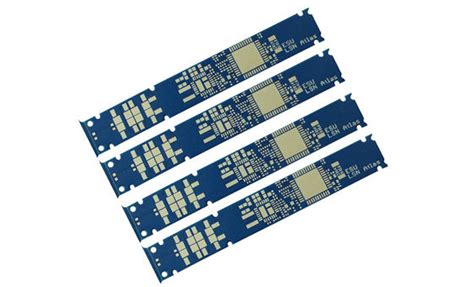
Sequential lamination is a process used in the manufacturing of printed circuit boards (PCBs) where multiple layers of the board are laminated together in a specific sequence. This technique allows for the creation of complex, high-density PCBs with improved electrical performance and reliability compared to traditional PCB manufacturing methods.
In sequential lamination, the PCB is built up layer by layer, with each layer being laminated separately before being combined with the others. This process enables the use of different materials and thicknesses for each layer, allowing for greater design flexibility and the ability to incorporate features such as embedded components and high-density interconnects (HDI).
Advantages of Sequential Lamination
There are several key advantages to using sequential lamination in PCB manufacturing:
-
Improved Electrical Performance: By laminating each layer separately, the dielectric thickness between layers can be precisely controlled, resulting in better impedance control and reduced signal loss.
-
Increased Reliability: Sequential lamination allows for the use of different materials in each layer, which can be optimized for specific functions such as heat dissipation or mechanical strength. This can lead to improved overall reliability of the PCB.
-
Greater Design Flexibility: With sequential lamination, designers have more freedom to incorporate complex features such as embedded components, blind and buried vias, and HDI structures.
-
Cost Reduction: Although the initial setup costs for sequential lamination may be higher than traditional methods, the ability to create high-density boards with fewer layers can lead to overall cost savings in terms of materials and processing time.

Sequential Lamination Process
The sequential lamination process typically involves the following steps:
-
Layer Preparation: Each layer of the PCB is designed and fabricated separately, with the necessary circuitry, vias, and other features.
-
Lamination: The individual layers are laminated together using heat and pressure, with a specific lamination sequence determined by the design requirements.
-
Drilling: After lamination, holes are drilled through the board for vias and component placement.
-
Plating: The drilled holes are plated with copper to create electrical connections between layers.
-
Etching: The outer layers of the PCB are etched to create the final circuitry pattern.
-
Surface Finishing: A surface finish, such as HASL or ENIG, is applied to the PCB to protect the copper and improve solderability.
Here’s a table summarizing the key steps in the sequential lamination process:
| Step | Description |
|---|---|
| Layer Preparation | Design and fabricate individual layers |
| Lamination | Laminate layers together in a specific sequence |
| Drilling | Drill holes for vias and component placement |
| Plating | Plate drilled holes with copper |
| Etching | Etch outer layers to create final circuitry |
| Surface Finishing | Apply surface finish for protection and solderability |

Trends in Sequential Lamination
As the demand for high-performance, high-density PCBs continues to grow, several trends have emerged in sequential lamination technology:
1. Advanced Materials
One of the key trends in sequential lamination is the use of advanced materials for improved performance and reliability. Some examples include:
-
Low-Dk/Df Materials: These materials have a low dielectric constant and dissipation factor, which helps to reduce signal loss and improve high-frequency performance.
-
High-Tg Materials: Materials with a high glass transition temperature (Tg) offer better thermal stability and resistance to deformation during the lamination process.
-
Halogen-Free Materials: As environmental concerns grow, there is an increasing demand for halogen-free materials that comply with regulations such as RoHS and REACH.
2. Embedded Components
Another trend in sequential lamination is the use of embedded components, where passive components such as resistors and capacitors are embedded within the layers of the PCB. This can help to reduce the overall size and weight of the board, as well as improve electrical performance by reducing the distance between components.
3. High-Density Interconnects (HDI)
HDI technology is becoming increasingly popular in sequential lamination, as it allows for the creation of high-density boards with fine pitch features. This is achieved through the use of microvias, which are small, laser-drilled holes that can be used to connect layers within the PCB.
4. Automation and Process Control
As with any manufacturing process, there is a trend towards increased automation and process control in sequential lamination. This includes the use of advanced lamination presses with precise temperature and pressure control, as well as automated optical inspection (AOI) systems for quality control.

Best Practices for Sequential Lamination
To ensure the success of a sequential lamination project, there are several best practices that should be followed:
-
Design for Manufacturability (DFM): It’s essential to design the PCB with manufacturability in mind, taking into account factors such as material selection, layer stackup, and via placement.
-
Material Selection: Choose materials that are compatible with the specific requirements of the project, such as thermal stability, electrical performance, and environmental compliance.
-
Process Control: Implement strict process controls to ensure consistency and quality throughout the lamination process, including temperature and pressure monitoring, and regular maintenance of equipment.
-
Testing and Inspection: Conduct thorough testing and inspection at each stage of the process to identify and correct any issues as early as possible.
-
Collaboration with Suppliers: Work closely with material suppliers and PCB manufacturers to ensure that all requirements are understood and met.
Frequently Asked Questions (FAQ)
-
Q: What is the difference between sequential lamination and traditional PCB lamination?
A: In traditional PCB lamination, all layers are laminated together at once, while in sequential lamination, each layer is laminated separately before being combined. This allows for greater design flexibility and the use of different materials in each layer. -
Q: What are the benefits of using embedded components in sequential lamination?
A: Embedded components can help to reduce the size and weight of the PCB, as well as improve electrical performance by reducing the distance between components. This can be particularly beneficial in applications where space is limited, such as in mobile devices or wearables. -
Q: What is HDI technology, and how is it used in sequential lamination?
A: HDI (High-Density Interconnect) technology refers to the use of microvias, which are small, laser-drilled holes that can be used to connect layers within the PCB. This allows for the creation of high-density boards with fine pitch features, which is becoming increasingly important in modern electronics. -
Q: What are some of the advanced materials used in sequential lamination?
A: Some examples of advanced materials used in sequential lamination include low-Dk/Df materials for improved high-frequency performance, high-Tg materials for better thermal stability, and halogen-free materials for environmental compliance. -
Q: What are some best practices for ensuring the success of a sequential lamination project?
A: Some best practices for sequential lamination include designing for manufacturability (DFM), selecting appropriate materials, implementing strict process controls, conducting thorough testing and inspection, and collaborating closely with material suppliers and PCB manufacturers.
Conclusion
Sequential lamination is a powerful technique for creating high-performance, high-density PCBs with improved electrical performance and reliability. By laminating each layer separately and using advanced materials and technologies such as embedded components and HDI, designers can create complex boards that meet the demands of modern electronics.
To ensure the success of a sequential lamination project, it’s essential to follow best practices such as DFM, material selection, process control, testing and inspection, and collaboration with suppliers. As the technology continues to evolve, we can expect to see even more advanced applications of sequential lamination in the future.


Leave a Reply