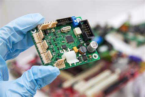
What is PCB Assembly?
PCB assembly is the process of soldering or mounting electronic components onto a printed circuit board (PCB). A PCB mechanically supports and electrically connects electronic components using conductive traces, pads and other features etched from one or more sheet layers of copper laminated onto and/or between sheet layers of a non-conductive substrate. Components are generally soldered onto the PCB to both electrically connect and mechanically fasten them to it.
PCB assembly can be done manually for simple prototypes and low-volume production, or by machine in a highly automated process for volume manufacturing. The main steps involved in PCB assembly include:
- Solder Paste Stenciling
- Pick and Place
- Reflow Soldering
- Inspection and Quality Control
Solder Paste Stenciling
The first step in PCB assembly is applying solder paste to the board. Solder paste is a gray, putty-like material that consists of tiny balls of solder suspended in flux. It is applied to the PCB using a stainless steel or polyester stencil that has openings corresponding to the pads on the board where components will be mounted.
The stencil is aligned on top of the PCB and solder paste is spread across it with a squeegee blade, forcing the paste through the openings and onto the pads below. The amount of solder paste deposited is controlled by the thickness of the stencil and the size of the openings.
After stenciling, the PCB is inspected to ensure proper solder paste coverage on all pads. If any defects like bridging, poor release, or insufficient solder are found, the board may need to be cleaned and the process repeated.
Pick and Place
With the solder paste applied, the PCB is ready for the components to be mounted. On an automated assembly line, this is done by a pick and place machine. The components, which come packaged in reels, trays, or tubes, are fed into the machine.
Using computer vision and precision nozzles, the machine rapidly picks up each component and places it onto the solder paste covered pads in its designated location on the PCB. Components can be placed at speeds up to tens of thousands per hour with modern machines. The machine also rotates components to the correct orientation as needed.
For manual assembly, a technician places each component by hand using tweezers and a magnifying lens. A paste dispenser may be used to apply solder paste to individual pads as the components are placed.
Reflow Soldering
After all the components are placed, the populated PCB is run through a reflow oven to permanently solder the parts. The oven has a conveyor belt that carries the board through several temperature zones that gradually heat it up to the soldering temperature, activate the flux to clean the component leads, melt the solder paste, and then cool the board back down to room temperature.
The entire process takes only a few minutes. The heat profile is carefully controlled for proper wetting of component leads without damaging any heat sensitive parts. Nitrogen gas is often used in the oven to improve solder joint quality and reduce oxidation.
After reflow, the solder solidifies, creating mechanical and electrical bonds between the component leads and the pads on the PCB. The PCB is now a functional electronic assembly.
Inspection and Quality Control
The assembled PCB goes through a variety of inspections and electrical tests to verify manufacturing quality before it can be shipped to the customer. Common inspection methods include:
- Visual Inspection: Looking for missing or misaligned components, solder defects, or board damage
- Automated Optical Inspection (AOI): Using cameras and image analysis to rapidly check component placement and solder joints
- X-Ray Inspection: Checking for voids, shorts, or opens in solder joints hidden under components
- In-Circuit Test (ICT): Probing test points to verify component values and proper connectivity
- Functional Test: Powering on the board and running test routines to ensure proper operation
Boards that fail inspection may be reworked if possible or scrapped if the defects can’t be corrected. Passing boards are cleaned of any residual flux, conformal coated if needed for environmental protection, and labeled before being packaged for shipping.
PCB Assembly Methods
There are several different methods used for PCB assembly depending on the components being mounted and the production volumes required. The most common are:
Through-Hole Assembly
Through-hole components have long metal leads that are inserted into plated holes drilled through the PCB. The leads are soldered to pads on the opposite side of the board, either by hand or using a wave soldering machine. Through-hole components are larger and heavier than surface mount parts and are mostly used on simpler, lower density boards. Examples include connectors, large capacitors, transformers, and power transistors.
Surface Mount Assembly
Surface mount components have small metal tabs or pins that are soldered directly onto pads on the surface of the PCB. No holes are required in the board, allowing parts to be mounted on both sides and packed closer together. Surface mount components are smaller and lighter than through-hole parts and are used on most modern high-density boards. Examples include chips, resistors, and small capacitors. Surface mount assembly is almost always done by machine, except for some prototypes and rework.
Mixed Assembly
Some PCBs use a mix of both through-hole and surface mount components. The surface mount parts are stenciled and placed first, then the board is flipped over for the through-hole parts to be inserted, and finally the whole assembly is soldered in one pass through the reflow oven or wave soldering machine. Wave soldering can be used after reflow since the surface mount parts are glued in place by the solidified solder paste.

PCB Assembly Equipment
A range of specialized equipment is used in electronics PCB assembly:
| Equipment | Description |
|---|---|
| Stencil Printer | Aligns PCB and stencil and applies solder paste |
| Pick and Place Machine | Mounts components onto PCB |
| Reflow Oven | Melts solder paste to permanently attach components |
| Wave Soldering Machine | Solders through-hole components on bottom of PCB |
| Automated Optical Inspection (AOI) | Checks component placement and solder joints |
| X-Ray Inspection | Finds defects in solder joints under components |
| In-Circuit Tester (ICT) | Probes test points to verify assembly electrically |
Other common equipment includes paste dispensers, board cleaners, labelers, and conveyors to move boards between machines. There is also an extensive variety of hand tools used such as tweezers, soldering irons, scrapers, flux pens, and magnifiers.

PCB Assembly Workstations
The facility and environment where PCB assembly is performed is important for efficiency, quality, and safety. Workstations need proper lighting, ventilation, and electrostatic discharge (ESD) protection.
ESD can instantly damage sensitive electronic components. Technicians must wear grounded wrist straps and work on grounded dissipative mats. Relative humidity needs to be controlled to minimize ESD risk.
Workstations are supplied with compressed air for pneumatic tools. Microscopes or magnifiers on articulated arms help with inspecting fine details. Fume extractors pull solder and solvent fumes away from technicians and filter the air.
Carts and racks are used to stage components and work in progress. Inventory must be managed to ensure parts are on hand when needed for a job but are not sitting around longer than necessary taking up space and capital. Proper shelving, environmental controls, and stock rotation maximize shelf life.

PCB Design for Assembly
How a PCB is designed has a big impact on the ease and cost of assembling it. Communication between the PCB designer and the assembly provider is critical to optimize the design for manufacturing (DFM).
Some key PCB design factors affecting assembly include:
- Component selection: Using readily available and proven components in standard packages
- Placement: Providing adequate spacing for pick and place nozzles
- Pad size: Making pads as large as practical to optimize solder joints
- Panelization: Laying out boards to be easily routed into panels that fit the assembly line
- Test points: Providing test points that are accessible for probing on ICT
- Fiducials: Including recognizable markings for machine vision alignment
- Solder mask: Opening up the solder mask around pads for better paste adhesion
PCB design software has automated checks for many assembly related factors and can generate files needed by the assembly provider. However, a thorough design review between the designer, assembler, and other stakeholders is still important to identify any issues and improvements early in the development cycle before boards are fabricated.
PCB Assembly Costs
The cost of PCB assembly is determined by the size and complexity of the board, the number and types of components, and the production volume. One-time setup costs like creating a stencil, programming machines, and generating test fixtures are amortized across the production run. So higher volumes generally have a lower per unit cost.
Costs can be reduced by following DFM guidelines to minimize the number of unique parts, use standard component packages, and avoid very tight tolerances beyond the capabilities of common assembly processes. Panelizing multiple boards into larger arrays reduces assembly time.
Procurement can be a substantial part of PCB assembly cost. Managing the supply chain to find the best component sources, track lead times, and react to shortages all factor into delivering on time and on budget. The cheapest assembly service is no good if boards can’t be built because of a lack of parts.
Quality is also a critical factor in PCB assembly cost. Higher quality may require more inspection and rework but reduces scrap and prevents costly warranty returns and damage to the end product’s reputation. The true cost of quality needs to be understood, not just the price paid to the assembler.
Choosing a PCB Assembly Provider
With so many factors involved in successful PCB assembly, carefully selecting the right provider is crucial. Some key considerations include:
- Technical capabilities: Can they handle the technologies and components used on the board?
- Capacity: Do they have enough equipment and staff to meet the needed volumes and deadlines?
- Quality system: What certifications, inspections, and tests do they use to ensure quality?
- Communication: Will they provide meaningful status updates and promptly answer questions?
- Location: Are they geographically close for easy site visits and fast shipments?
- References: Do they have positive feedback from customers with similar needs?
Visiting the provider’s facility, meeting their team, and building a relationship over time provides the best information to make a selection. The right assembly provider is as invested in the end product’s success as the designer and becomes a trusted partner, not just a vendor.
Future of PCB Assembly
As electronics continue to spread into more products, the demand for PCB assembly keeps growing. The most influential trends shaping the future of PCB assembly include:
- Miniaturization: Boards are getting smaller and denser, requiring more precise equipment and handling
- Advanced packaging: Newer component form factors like quad-flat no-leads (QFNs) and ball grid arrays (BGAs) are becoming more common
- High mix, low volume: Customization and faster product cycles are driving a shift away from mass production toward more frequent changeovers
- Automation: More sophisticated machine vision, robots, and ovens allow more of the assembly process to be automated
- Reshoring: Geopolitical uncertainty, tariffs, and intellectual property risks are causing some manufacturing to move closer to the engineering teams and end markets
One thing is certain – there is a bright future for those with the skills and experience to design and assemble PCBs. Electronics are essential to modern life and that is not going to change any time soon.
PCB Assembly FAQ
Q: What is the difference between PCB assembly and PCB fabrication?
A: PCB fabrication is the process of making the bare printed circuit board, while PCB assembly is the process of soldering components onto the fabricated board. PCB fabrication is done by a separate provider prior to assembly.
Q: How long does PCB assembly take?
A: Assembly time depends on the complexity of the board and the production volume. Simple boards in small quantities might be assembled in a few days, while complex boards in high volumes could take several weeks. Consult with the provider on their lead times for a specific job.
Q: What standards are used for PCB assembly?
A: The most widely used standards are IPC-A-610 for acceptability of electronic assemblies and J-STD-001 for soldered electrical and electronic assemblies. These define workmanship criteria, inspection methods, and defect classifications to ensure consistency across the industry.
Q: What file formats are needed for PCB assembly?
A: The most common file formats are Gerber RS-274X for the board fabrication data, Excellon for drilling data, and CSV (comma separated values) for the bill of materials and component positions. These are all text-based formats that can be generated by most PCB design software. Some providers may also accept 3D files in STEP format to help with quoting and planning.
Q: How much does PCB assembly cost?
A: PCB assembly costs can range from tens of dollars to thousands of dollars or more, depending on the board size, number of components, volumes, and turnaround time. The best way to get an accurate quote is to provide the fabrication and bill of material files to the provider for evaluation. They can usually give a detailed quote broken down by setup costs, part costs, and assembly labor.


Leave a Reply