Introduction to PCB Routing Practices
Printed Circuit Board (PCB) routing is a critical aspect of electronic design that involves connecting various components on a board using conductive traces. Proper PCB routing practices ensure the reliability, functionality, and manufacturability of the final product. In this article, we will explore the top 10 best PCB routing practices that every designer should follow to achieve optimal results.
What is PCB Routing?
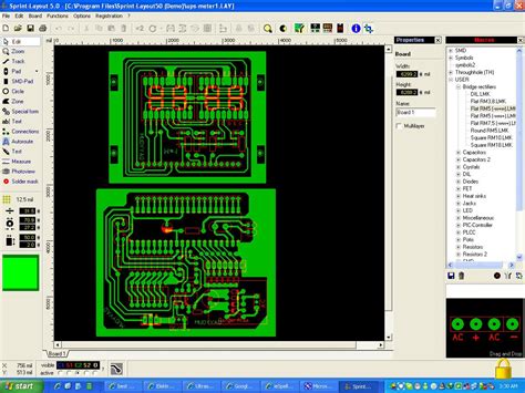
PCB routing refers to the process of creating electrical connections between components on a printed circuit board using conductive traces, vias, and planes. The goal of PCB routing is to ensure that signals are transmitted efficiently and reliably while minimizing interference and signal integrity issues.
Why are PCB Routing Practices Important?
Following best PCB routing practices is essential for several reasons:
-
Signal Integrity: Proper routing techniques minimize signal distortion, crosstalk, and electromagnetic interference (EMI), ensuring that signals reach their intended destinations without degradation.
-
Manufacturability: Well-designed PCB layouts are easier to manufacture, reducing the chances of defects and improving yield rates.
-
Reliability: Optimal routing practices enhance the reliability of the final product by minimizing stress on components and connections, reducing the risk of failures.
-
Cost-effectiveness: Efficient PCB routing can help reduce manufacturing costs by optimizing board space and minimizing the need for expensive materials or processes.
Top 10 Best PCB Routing Practices
1. Plan Your Layout
Before starting the routing process, it is crucial to plan your PCB layout carefully. Consider the following factors:
- Component placement
- Power distribution
- Signal flow
- Mechanical constraints
A well-planned layout provides a solid foundation for efficient routing and helps avoid potential issues down the line.
2. Use a Ground Plane
Incorporating a ground plane in your PCB design offers several benefits:
- Reduces EMI and crosstalk
- Provides a low-impedance return path for signals
- Helps maintain signal integrity
- Improves thermal management
When using a ground plane, ensure that it covers as much of the board as possible and is properly connected to the components’ ground pins.
3. Minimize Trace Length
Keeping trace lengths as short as possible is essential for several reasons:
- Reduces signal delay and attenuation
- Minimizes the risk of EMI and crosstalk
- Improves signal integrity
- Saves board space
To minimize trace length, place components strategically and use direct routes whenever possible.
4. Match Trace Impedance
Matching trace impedance is crucial for high-speed signals to maintain signal integrity and minimize reflections. To achieve impedance matching:
- Calculate the required trace width and spacing based on the board’s dielectric properties and the desired impedance.
- Use a PCB design tool that supports impedance control features.
- Work closely with your PCB manufacturer to ensure that the specified impedance requirements are met.
5. Avoid Sharp Angles
Sharp angles in traces can cause signal reflection and EMI issues. To minimize these problems:
- Use 45-degree angles instead of 90-degree angles when changing trace direction.
- Implement curved traces or chamfered corners for smoother transitions.
- Avoid creating acute angles between traces and pads.
6. Provide Adequate Clearance
Maintaining sufficient clearance between traces, components, and board edges is essential for several reasons:
- Prevents short circuits and arcing
- Facilitates manufacturing processes, such as soldering and inspection
- Reduces the risk of signal interference
- Ensures compliance with safety standards
Consult your PCB manufacturer’s design guidelines for recommended clearance values.
7. Use Via Stitching for High-Speed Signals
Via stitching is a technique that involves placing vias along the edges of a high-speed signal trace to create a Faraday cage-like structure. This practice offers several benefits:
- Minimizes EMI radiation from the trace
- Provides a low-impedance return path for the signal
- Improves signal integrity and reduces crosstalk
When implementing via stitching, ensure that the vias are placed close enough to the trace to be effective without causing manufacturing issues.
8. Route Differential Pairs Carefully
Differential signaling is commonly used in high-speed digital interfaces, such as USB, HDMI, and PCI Express. When routing differential pairs:
- Keep the traces close together to maintain signal integrity and minimize EMI.
- Match the length of the traces to ensure that the signals arrive at the receiver simultaneously.
- Avoid routing differential pairs near other high-speed traces or noisy components.
- Use your PCB design tool’s differential pair routing features to simplify the process.
9. Optimize Power Distribution
Proper power distribution is crucial for the stability and performance of your PCB. To optimize power distribution:
- Use dedicated power planes or wide traces to minimize voltage drop and improve current-carrying capacity.
- Place decoupling capacitors close to power-hungry components to reduce noise and maintain a stable supply voltage.
- Separate analog and digital power supplies to minimize interference.
- Use power and ground plane fills to provide low-impedance paths for return currents.
10. Perform Design Rule Checks (DRC)
Before finalizing your PCB layout, perform thorough Design Rule Checks (DRC) to ensure that your design adheres to the manufacturer’s specifications and industry standards. DRC helps identify potential issues, such as:
- Insufficient clearance between traces and components
- Violation of minimum trace width and spacing requirements
- Missing or incorrect connections
- Unintended short circuits
Most PCB design tools have built-in DRC features that automate the checking process, saving time and reducing the risk of errors.

Frequently Asked Questions (FAQ)
1. What is the difference between a trace and a via?
A trace is a conductive path that connects components on the same layer of a PCB, while a via is a conductive hole that connects traces on different layers.
2. How do I determine the appropriate trace width for my design?
The appropriate trace width depends on several factors, such as the required current-carrying capacity, the desired impedance, and the PCB manufacturer’s capabilities. Consult your PCB manufacturer’s design guidelines and use online calculators or your PCB design tool’s features to determine the optimal trace width.
3. What is the purpose of a ground plane in PCB routing?
A ground plane serves as a low-impedance reference point for signals, helping to maintain signal integrity, reduce EMI and crosstalk, and improve thermal management.
4. Why is it important to match trace lengths in differential pairs?
Matching trace lengths in differential pairs ensures that the signals arrive at the receiver simultaneously, minimizing signal skew and maintaining signal integrity.
5. How can I minimize EMI in my PCB design?
To minimize EMI in your PCB design, use a ground plane, implement proper shielding, route high-speed signals away from sensitive components, use via stitching for critical traces, and adhere to recommended clearance and spacing guidelines.

Conclusion
Following best PCB routing practices is essential for creating reliable, high-performance electronic products. By planning your layout carefully, using a ground plane, minimizing trace lengths, matching impedances, avoiding sharp angles, providing adequate clearance, using via stitching for high-speed signals, routing differential pairs carefully, optimizing power distribution, and performing thorough Design Rule Checks, you can ensure that your PCB design meets the highest standards of quality and functionality.
Remember to consult your PCB manufacturer’s design guidelines and work closely with their engineering team to ensure that your design is manufacturable and cost-effective. By adhering to these top 10 best PCB routing practices, you can streamline your design process, reduce the risk of errors, and ultimately create better electronic products.
| Practice | Benefit |
|---|---|
| Plan Your Layout | Provides a solid foundation for efficient routing and helps avoid potential issues |
| Use a Ground Plane | Reduces EMI and crosstalk, provides a low-impedance return path, improves signal integrity and thermal management |
| Minimize Trace Length | Reduces signal delay and attenuation, minimizes EMI and crosstalk, improves signal integrity, saves board space |
| Match Trace Impedance | Maintains signal integrity and minimizes reflections for high-speed signals |
| Avoid Sharp Angles | Minimizes signal reflection and EMI issues |
| Provide Adequate Clearance | Prevents short circuits and arcing, facilitates manufacturing processes, reduces signal interference, ensures compliance with safety standards |
| Use Via Stitching for High-Speed Signals | Minimizes EMI radiation, provides a low-impedance return path, improves signal integrity and reduces crosstalk |
| Route Differential Pairs Carefully | Maintains signal integrity, minimizes EMI, ensures signals arrive simultaneously at the receiver |
| Optimize Power Distribution | Minimizes voltage drop, improves current-carrying capacity, reduces noise, maintains stable supply voltage |
| Perform Design Rule Checks (DRC) | Ensures design adheres to manufacturer’s specifications and industry standards, identifies potential issues |
By incorporating these top 10 best PCB routing practices into your design workflow, you can create high-quality, reliable, and manufacturable PCBs that meet the demands of today’s complex electronic products.


Leave a Reply