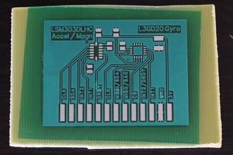
What is PCB Soldermask?
PCB soldermask, also known as solder resist or solder mask, is a protective coating applied to the copper traces of a printed circuit board (PCB) to prevent short circuits and oxidation. It is a thin layer of polymer that covers the copper traces, leaving only the areas that need to be soldered exposed. The soldermask also provides a visual reference for the placement of components and helps to improve the overall aesthetics of the PCB.
Types of PCB Soldermask
There are two main types of soldermask used in PCB manufacturing:
-
Liquid Photoimageable Soldermask (LPI): This type of soldermask is applied as a liquid and then exposed to UV light through a photomask to create the desired pattern. LPI soldermask is the most common type used in PCB manufacturing due to its high resolution and durability.
-
Dry Film Soldermask (DFM): This type of soldermask is applied as a dry film and then laminated onto the PCB surface. DFM soldermask is less common than LPI soldermask but is still used in some applications due to its ease of application and lower cost.
Why is Testing PCB Soldermask Important?
Testing PCB soldermask is crucial to ensure the quality and reliability of the finished PCB. Some of the reasons why testing soldermask is important include:
-
Preventing short circuits: Soldermask acts as an insulator between the copper traces, preventing short circuits that can cause the PCB to malfunction or fail.
-
Improving solderability: Soldermask helps to control the flow of solder during the soldering process, ensuring that the solder only adheres to the exposed areas of the copper traces.
-
Enhancing durability: Soldermask provides a protective layer that helps to prevent oxidation and corrosion of the copper traces, improving the overall durability of the PCB.
-
Ensuring consistent quality: Testing soldermask helps to ensure that the finished PCB meets the required specifications and quality standards, reducing the risk of defects and failures.

Methods for Testing PCB Soldermask
There are several methods used to test PCB soldermask, each with its own advantages and limitations. Some of the most common methods include:
1. Visual Inspection
Visual inspection is the most basic method for testing PCB soldermask. It involves visually examining the PCB under magnification to check for defects such as pinholes, scratches, or contamination. Visual inspection is a quick and easy method but is limited by the resolution of the human eye and may not detect smaller defects.
2. Thickness Measurement
Thickness measurement involves using a micrometer or other measurement tool to measure the thickness of the soldermask layer. This method is used to ensure that the soldermask is applied evenly and to the correct thickness specified in the PCB design. Thickness measurement is a simple and reliable method but may not detect other types of defects.
3. Adhesion Testing
Adhesion testing involves applying a force to the soldermask layer to test its adhesion to the copper traces. This can be done using a tape test, where a piece of tape is applied to the soldermask and then peeled off to see if any of the soldermask comes off with the tape. Adhesion testing is important to ensure that the soldermask will not peel or flake off during the assembly process or in use.
4. Electrical Testing
Electrical testing involves applying a voltage to the PCB and measuring the resistance between the copper traces. This method is used to ensure that the soldermask is providing adequate insulation and preventing short circuits. Electrical testing is a more comprehensive method than visual inspection or thickness measurement but requires specialized equipment and expertise.
5. Chemical Resistance Testing
Chemical resistance testing involves exposing the soldermask to various chemicals such as solvents, acids, or bases to test its resistance to these substances. This method is important for PCBs that will be used in harsh environments or exposed to chemicals during the manufacturing process. Chemical resistance testing requires specialized equipment and expertise and may be destructive to the PCB.

Factors Affecting PCB Soldermask Quality
Several factors can affect the quality of PCB soldermask, including:
-
Material selection: The type of soldermask material used can affect its performance and durability. LPI soldermask is generally considered to be the highest quality but may be more expensive than other types.
-
Application method: The method used to apply the soldermask can affect its thickness, adhesion, and coverage. LPI soldermask is typically applied using screen printing or spray coating, while DFM soldermask is laminated onto the PCB surface.
-
Curing process: The curing process used to harden the soldermask can affect its durability and resistance to chemicals and environmental factors. Proper curing is essential to ensure that the soldermask achieves its full strength and stability.
-
Handling and storage: Improper handling or storage of the PCB can cause damage to the soldermask, such as scratches or contamination. It is important to handle PCBs with care and store them in a clean, dry environment.

Best Practices for Testing PCB Soldermask
To ensure the highest quality and reliability of PCB soldermask, it is important to follow best practices for testing and inspection. Some of these best practices include:
-
Establish clear specifications: Before testing, it is important to establish clear specifications for the soldermask, including thickness, adhesion, and chemical resistance requirements. These specifications should be based on the intended use and environment of the PCB.
-
Use multiple testing methods: No single testing method can detect all types of defects or ensure complete coverage. It is important to use a combination of visual inspection, thickness measurement, adhesion testing, electrical testing, and chemical resistance testing to ensure comprehensive coverage.
-
Document results: All testing results should be carefully documented and reviewed to identify any issues or areas for improvement. Documentation should include the type of test performed, the results obtained, and any corrective actions taken.
-
Implement process controls: To ensure consistent quality, it is important to implement process controls throughout the PCB manufacturing process. This includes controlling the soldermask application process, curing process, and handling and storage procedures.
-
Continuously monitor and improve: Testing and inspection should be an ongoing process, with continuous monitoring and improvement to identify and address any issues that arise. Regular audits and reviews can help to identify areas for improvement and ensure that best practices are being followed.
Common PCB Soldermask Defects and Their Causes
Despite best efforts, PCB soldermask defects can still occur. Some of the most common defects and their causes include:
-
Pinholes: Pinholes are small holes or voids in the soldermask that can expose the underlying copper traces. Pinholes can be caused by contamination, improper curing, or damage during handling.
-
Scratches: Scratches in the soldermask can expose the underlying copper traces and compromise the insulation properties of the soldermask. Scratches can be caused by improper handling, debris, or damage during the manufacturing process.
-
Contamination: Contamination of the soldermask can occur due to improper cleaning, handling, or storage. Contaminants can include dirt, dust, oils, or other substances that can interfere with the adhesion or curing of the soldermask.
-
Uneven thickness: Uneven thickness of the soldermask can compromise its insulation properties and lead to short circuits or other defects. Uneven thickness can be caused by improper application, curing, or handling.
-
Poor adhesion: Poor adhesion of the soldermask to the copper traces can cause the soldermask to peel or flake off, exposing the underlying copper. Poor adhesion can be caused by contamination, improper curing, or incompatible materials.
Frequently Asked Questions (FAQ)
-
What is the difference between LPI and DFM soldermask?
LPI (Liquid Photoimageable) soldermask is applied as a liquid and then exposed to UV light to create the desired pattern, while DFM (Dry Film) soldermask is applied as a dry film and then laminated onto the PCB surface. LPI soldermask is generally considered to be higher quality and more durable than DFM soldermask. -
How thick should PCB soldermask be?
The thickness of PCB soldermask can vary depending on the specific application and requirements of the PCB. Typically, Soldermask Thickness ranges from 0.5 to 2.0 mils (12.7 to 50.8 microns). The thickness should be specified in the PCB design and carefully controlled during the manufacturing process. -
Can PCB soldermask be repaired if damaged?
In some cases, minor damage to PCB soldermask can be repaired using specialized repair kits or techniques. However, more extensive damage may require the PCB to be scrapped and replaced. It is always best to prevent damage through proper handling and storage procedures. -
How can I test the chemical resistance of PCB soldermask?
Chemical resistance testing involves exposing the soldermask to various chemicals such as solvents, acids, or bases to test its resistance to these substances. This can be done using specialized equipment and procedures, such as immersion testing or exposure to chemical vapors. The specific chemicals and exposure times will depend on the intended use and environment of the PCB. -
What are the most common causes of PCB soldermask defects?
The most common causes of PCB soldermask defects include contamination, improper curing, uneven thickness, poor adhesion, and damage during handling or storage. These defects can be prevented through careful process control, handling, and storage procedures, as well as regular testing and inspection to identify and address any issues that arise.
Conclusion
PCB soldermask is a critical component of PCB manufacturing that provides insulation, protection, and improved solderability to the copper traces. Testing PCB soldermask is essential to ensure the quality and reliability of the finished PCB and to prevent defects and failures. There are several methods for testing PCB soldermask, including visual inspection, thickness measurement, adhesion testing, electrical testing, and chemical resistance testing. To ensure the highest quality and reliability, it is important to follow best practices for testing and inspection, including establishing clear specifications, using multiple testing methods, documenting results, implementing process controls, and continuously monitoring and improving the process. By understanding the importance of PCB soldermask testing and following best practices, PCB manufacturers can ensure the highest quality and reliability of their products.


Leave a Reply