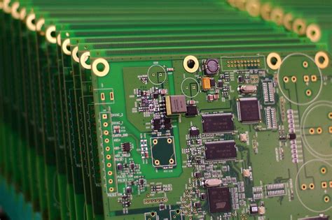
Introduction to PCB Assembly
PCB assembly is the process of assembling electronic components onto a printed circuit board (PCB) to create a functional electronic device. The PCB serves as the foundation for the electronic components and provides the necessary electrical connections between them. The assembly process involves several steps, including component placement, soldering, inspection, and testing.
Key Steps in PCB Assembly
- Solder Paste Application
- Component Placement
- Reflow Soldering
- Inspection and Testing
- Final Assembly and Packaging
Preparing for PCB Assembly
Before starting the PCB assembly process, it is essential to ensure that all necessary materials and equipment are available and properly prepared.
Materials Required
- Printed Circuit Board (PCB)
- Electronic Components
- Solder Paste
- Solder Wire
- Flux
- Cleaning Agents
Equipment Needed
- Pick and Place Machine
- Reflow Oven
- Soldering Iron
- Inspection Microscope
- Testing Equipment
PCB Design Considerations
To facilitate a smooth assembly process, the PCB design should adhere to certain guidelines:
- Ensure proper component footprints and pad sizes
- Maintain appropriate spacing between components
- Provide clear silkscreen markings for Component Orientation
- Include Fiducial Markers for machine vision alignment

Solder Paste Application
Solder paste is a mixture of tiny solder particles suspended in a flux medium. It is applied to the PCB pads to provide a temporary adhesive for the components and to enable soldering during the reflow process.
Solder Paste Printing Methods
- Stencil Printing
- Most common method for high-volume production
- Utilizes a stainless steel stencil with apertures corresponding to the PCB pads
-
Solder paste is spread over the stencil and onto the PCB using a squeegee
-
Dispensing
- Suitable for low-volume or prototype production
- Solder paste is dispensed onto the PCB pads using a pneumatic or mechanical dispenser
- Offers flexibility for custom designs or rework
Solder Paste Inspection
After applying the solder paste, it is crucial to inspect the PCB to ensure proper paste deposition. Inspection methods include:
- Visual Inspection: Checking for consistent paste volume, alignment, and absence of bridging or voids
- Automated Optical Inspection (AOI): Using machine vision systems to detect paste deposition defects
- 3D Solder Paste Inspection (SPI): Utilizing laser scanning to measure paste volume and height

Component Placement
Component placement involves positioning and orienting the electronic components onto the PCB pads with the applied solder paste.
Types of Component Placement
- Surface Mount Technology (SMT)
- Components are placed directly onto the PCB surface
- Requires precise placement and orientation
-
Enables high-density designs and smaller form factors
-
Through-Hole Technology (THT)
- Components have leads that are inserted through holes in the PCB
- Provides stronger mechanical connections
- Suitable for larger components or high-power applications
Pick and Place Machines
Pick and place machines automate the component placement process, especially for SMT components.
| Machine Type | Placement Speed (cph) | Accuracy (μm) | Suitable for |
|---|---|---|---|
| High-Speed | 80,000 – 200,000 | ±50 | High-volume production |
| Mid-Range | 20,000 – 80,000 | ±50 | Medium-volume production |
| Benchtop | 5,000 – 20,000 | ±100 | Low-volume or prototype production |
cph = components per hour
These machines use machine vision to locate and align components, vacuum nozzles to pick up components, and precise motion control to place them accurately on the PCB.
Manual Placement
For low-volume production or prototype assembly, manual placement of components using tweezers or vacuum pens is common. This method is more time-consuming and requires skilled operators to ensure accurate placement and orientation.

Reflow Soldering
Reflow soldering is the process of heating the PCB and components to melt the solder paste and form permanent electrical and mechanical connections.
Reflow Oven Temperature Profile
The reflow oven temperature profile consists of several stages:
- Preheat: Gradually raises the temperature to activate the flux and remove solvents
- Soak: Maintains a stable temperature to ensure even heating of the PCB and components
- Reflow: Increases the temperature above the solder melting point to form solder joints
- Cooling: Gradually cools the PCB to solidify the solder joints
A typical reflow temperature profile for lead-free solder is shown below:
| Stage | Temperature (°C) | Time (seconds) |
|---|---|---|
| Preheat | 25 – 150 | 60 – 120 |
| Soak | 150 – 180 | 60 – 120 |
| Reflow | 220 – 250 | 30 – 60 |
| Cooling | 250 – 25 | 60 – 120 |
Reflow Oven Types
- Convection Reflow Oven
- Uses hot air circulation to heat the PCB and components
- Provides even heating and consistent solder joint formation
-
Suitable for high-volume production
-
Infrared (IR) Reflow Oven
- Utilizes infrared radiation to heat the PCB and components
- Offers rapid heating and shorter reflow cycles
-
Requires careful control to prevent overheating of sensitive components
-
Vapor Phase Reflow Oven
- Uses a heated vapor to transfer heat to the PCB and components
- Provides uniform heating and reduces the risk of thermal damage
- Suitable for assembly of high-density or thermally sensitive components
Inspection and Testing
After the reflow soldering process, it is essential to inspect and test the assembLED PCB to ensure quality and functionality.
Visual Inspection
Visual inspection involves examining the solder joints, component placement, and overall PCB condition. Inspection criteria include:
- Solder joint appearance: Smooth, shiny, and properly formed fillets
- Component alignment and orientation
- Absence of defects such as bridging, tombstoning, or insufficient solder
Automated Optical Inspection (AOI)
AOI systems use machine vision to automatically detect assembly defects. These systems compare the assembled PCB to a reference image and highlight any discrepancies. AOI can detect issues such as:
- Missing or misaligned components
- Solder joint defects (bridging, insufficient solder, etc.)
- Polarity or orientation errors
X-Ray Inspection
X-ray inspection is used to examine solder joints and components that are not visible from the surface, such as ball grid array (BGA) packages or hidden joints. X-ray systems can detect:
- Solder joint voids or cracks
- Insufficient or excessive solder
- Component placement and alignment issues
Electrical Testing
Electrical testing verifies the functionality and performance of the assembled PCB. Common testing methods include:
- In-Circuit Testing (ICT)
- Uses a bed-of-nails fixture to make electrical contact with test points on the PCB
-
Performs tests such as continuity, resistance, capacitance, and voltage measurements
-
Functional Testing
- Applies input signals to the PCB and measures output responses
-
Verifies the PCB’s functionality under various operating conditions
-
Boundary Scan Testing
- Utilizes built-in test circuitry (JTAG) to test interconnections and components
- Suitable for testing complex digital circuits and identifying faults
Final Assembly and Packaging
After inspection and testing, the assembled PCBs undergo final assembly and packaging steps.
Final Assembly
Final assembly may include:
- Attaching heat sinks or thermal management components
- Mounting the PCB into an enclosure or chassis
- Connecting wires, cables, or connectors
- Applying conformal coating for environmental protection
Packaging and Shipping
Proper packaging ensures that the assembled PCBs are protected during storage and transportation. Packaging considerations include:
- Electrostatic discharge (ESD) protection
- Moisture barrier bags or desiccants to prevent humidity damage
- Padding or cushioning materials to prevent physical damage
- Labeling and documentation for traceability and identification
Frequently Asked Questions (FAQ)
- What is the difference between SMT and THT component placement?
-
SMT (Surface Mount Technology) components are placed directly onto the PCB surface, while THT (Through-Hole Technology) components have leads that are inserted through holes in the PCB. SMT allows for higher-density designs and smaller form factors, while THT provides stronger mechanical connections and is suitable for larger components or high-power applications.
-
What is solder paste, and how is it applied to the PCB?
-
Solder paste is a mixture of tiny solder particles suspended in a flux medium. It is applied to the PCB pads to provide a temporary adhesive for the components and to enable soldering during the reflow process. Solder paste can be applied using stencil printing for high-volume production or dispensing for low-volume or prototype production.
-
What is the purpose of reflow soldering, and what are the different types of reflow ovens?
-
Reflow soldering is the process of heating the PCB and components to melt the solder paste and form permanent electrical and mechanical connections. The three main types of reflow ovens are convection (using hot air circulation), infrared (using infrared radiation), and vapor phase (using a heated vapor). Each type has its advantages and is suitable for different production requirements.
-
Why is inspection and testing important after the reflow soldering process?
-
Inspection and testing after reflow soldering are crucial to ensure the quality and functionality of the assembled PCB. Visual inspection, automated optical inspection (AOI), X-ray inspection, and electrical testing methods help detect defects, verify proper component placement and soldering, and confirm the PCB’s performance under various operating conditions.
-
What are the considerations for final assembly and packaging of the assembled PCBs?
- Final assembly may include attaching heat sinks, mounting the PCB into an enclosure, connecting wires or cables, and applying conformal coating for protection. Proper packaging is essential to protect the assembled PCBs during storage and transportation. Packaging considerations include ESD protection, moisture barrier bags, padding materials, and labeling for traceability and identification.


Leave a Reply