Understanding the Importance of Soldermask CTI in PCB Manufacturing
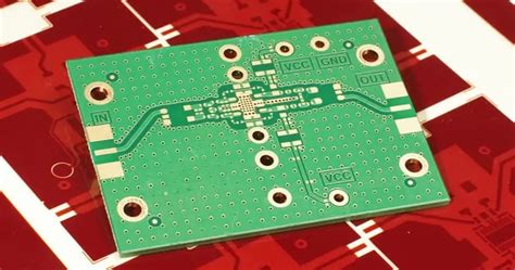
In the world of printed circuit board (PCB) manufacturing, the soldermask plays a crucial role in ensuring the reliability and longevity of the final product. Soldermask, also known as solder resist or solder mask, is a thin layer of polymer applied to the copper traces of a PCB to protect them from oxidation, prevent solder bridges, and provide electrical insulation. One of the key properties of soldermask that determines its performance in high-voltage applications is its Comparative Tracking Index (CTI).
What is Comparative Tracking Index (CTI)?
Comparative Tracking Index (CTI) is a measure of a material’s ability to resist electrical tracking and erosion when exposed to high-voltage stress and environmental contaminants. Tracking occurs when an electrical current creates a conductive path across an insulating surface, leading to a short circuit or other electrical failure. The higher the CTI value, the better the material’s resistance to tracking.
The CTI of a soldermask is determined by standardized testing methods, such as the IEC 60112 or ASTM D3638. In these tests, a sample of the soldermask material is subjected to a series of voltage stresses under controlled environmental conditions. The voltage at which tracking occurs is recorded, and the CTI value is assigned based on a predefined scale.
| CTI Range | Voltage Class |
|---|---|
| 600 ≤ CTI | 600 |
| 400 ≤ CTI < 600 | 400 |
| 175 ≤ CTI < 400 | 175 |
| 100 ≤ CTI < 175 | 100 |
The Significance of High CTI Soldermask in PCB Applications
High CTI soldermask is essential for PCBs used in applications that involve high voltages, such as power supplies, automotive electronics, and industrial control systems. In these applications, the soldermask must provide reliable insulation and prevent tracking, even in the presence of environmental contaminants like dust, moisture, and chemical pollutants.
Using a soldermask with a high CTI value offers several benefits:
-
Improved electrical safety: A high CTI soldermask reduces the risk of electrical shorts, arcing, and other hazards that can compromise the safety of the PCB and the device it powers.
-
Enhanced reliability: By resisting tracking and erosion, a high CTI soldermask helps maintain the integrity of the PCB’s copper traces over time, reducing the likelihood of premature failure.
-
Compliance with industry standards: Many industries have specific requirements for the CTI of soldermask used in their products. For example, the automotive industry often requires a minimum CTI of 400 for PCBs used in vehicles.
Factors Affecting Soldermask CTI
Several factors can influence the CTI of a soldermask, including:
Soldermask Material Composition
The chemical composition of the soldermask material plays a significant role in determining its CTI. Soldermasks are typically made from polymers such as epoxy, acrylic, or polyimide, each with its own set of properties and performance characteristics.
Epoxy-based soldermasks are the most common and offer good electrical insulation, chemical resistance, and adhesion to the PCB substrate. However, their CTI values are generally lower compared to other materials.
Acrylic soldermasks have excellent thermal and UV resistance, making them suitable for outdoor applications. They also have good electrical insulation properties and can achieve higher CTI values than epoxy-based soldermasks.
Polyimide soldermasks are known for their exceptional thermal stability, chemical resistance, and high CTI values. They are often used in high-reliability applications, such as aerospace and military electronics.
Soldermask Thickness
The thickness of the soldermask layer can also affect its CTI performance. A thicker soldermask provides better insulation and reduces the risk of pinholes or other defects that can compromise its tracking resistance. However, increasing the soldermask thickness can also impact the PCB’s manufacturability and cost.
Typical soldermask thicknesses range from 0.5 mil (12.7 μm) to 2 mil (50.8 μm), depending on the application and the soldermask material used. For high CTI applications, a minimum thickness of 1 mil (25.4 μm) is often recommended.
Surface Finish and Cleanliness
The surface finish of the PCB and the cleanliness of the soldermask can also influence its CTI performance. A smooth, uniform surface finish helps ensure consistent soldermask coverage and reduces the risk of defects that can lead to tracking.
Contamination of the soldermask surface by flux residues, dust, or other particles can create a path for tracking and reduce the CTI of the soldermask. Proper cleaning and inspection of the PCB during manufacturing are essential to maintain the soldermask’s CTI performance.
Selecting the Right Soldermask for High CTI Applications
When choosing a soldermask for high CTI applications, several factors should be considered:
-
CTI requirements: Determine the minimum CTI value required for your application based on industry standards, customer specifications, or the operating environment of the PCB.
-
Soldermask material: Select a soldermask material that meets or exceeds the required CTI value while also providing other necessary properties, such as thermal stability, chemical resistance, and adhesion to the PCB substrate.
-
Soldermask thickness: Specify a soldermask thickness that provides adequate insulation and tracking resistance for your application, taking into account the manufacturability and cost implications.
-
Surface finish and cleanliness: Ensure that the PCB manufacturing process includes proper surface preparation, soldermask application, and cleaning steps to maintain the soldermask’s CTI performance.
-
Supplier expertise: Work with a PCB manufacturer that has experience in producing high CTI boards and can provide guidance on soldermask selection, design, and testing.

Designing PCBs for High CTI Soldermask
When designing PCBs for high CTI applications, several best practices can help ensure optimal soldermask performance:
Copper Trace Spacing
Increasing the spacing between copper traces can help reduce the risk of tracking and improve the soldermask’s CTI performance. The minimum spacing should be based on the voltage requirements of the application and the CTI value of the soldermask.
| Voltage (V) | Minimum Spacing (mm) |
|---|---|
| ≤ 50 | 0.1 |
| 50 – 100 | 0.2 |
| 100 – 150 | 0.3 |
| 150 – 300 | 0.5 |
| > 300 | 1.0 |
Soldermask Openings
Minimizing the size of soldermask openings around component pads and vias can help reduce the exposure of the copper traces to environmental contaminants and improve the soldermask’s CTI performance. However, the openings must still be large enough to allow for proper soldering and inspection.
Soldermask Dams
Incorporating soldermask dams between closely spaced copper traces can provide additional insulation and tracking resistance. Soldermask dams are narrow strips of soldermask that separate adjacent traces and help prevent Solder Bridging during assembly.
Via Tenting
Tenting vias with soldermask can help prevent contamination and improve the soldermask’s CTI performance. Via tenting involves covering the via holes with soldermask on one or both sides of the PCB, depending on the application requirements.
Conformal Coating
In some cases, applying a conformal coating over the soldermask can provide additional protection against environmental contaminants and improve the PCB’s overall insulation and tracking resistance. Conformal Coatings are thin layers of polymer, such as acrylic, silicone, or urethane, that conform to the PCB’s surface and fill in any gaps or voids in the soldermask.
Testing and Qualification of High CTI Soldermask
To ensure that the soldermask meets the required CTI performance, PCBs should undergo testing and qualification according to industry standards and customer specifications. Some common tests for high CTI soldermask include:
-
CTI testing: Performed according to IEC 60112 or ASTM D3638 to determine the soldermask’s CTI value.
-
Insulation resistance testing: Measures the soldermask’s ability to resist current flow between conductors at a specified voltage.
-
Dielectric withstanding voltage (DWV) testing: Applies a high voltage between conductors to ensure that the soldermask can withstand the required voltage without breakdown.
-
Environmental testing: Exposes the PCB to various environmental conditions, such as temperature cycling, humidity, and salt spray, to evaluate the soldermask’s performance under real-world conditions.
Proper documentation of the testing and qualification process, including test reports and certificates of compliance, is essential to demonstrate that the PCB meets the required CTI performance and to support customer audits and regulatory compliance.
FAQ
1. What is the minimum CTI value required for high-voltage applications?
The minimum CTI value required for high-voltage applications depends on the specific industry and application requirements. In general, a CTI value of 400 or higher is considered suitable for most high-voltage applications. However, some industries, such as automotive and aerospace, may have more stringent requirements.
2. Can a high CTI soldermask be applied to any PCB substrate material?
High CTI soldermasks can be applied to most common PCB Substrate Materials, such as FR-4, polyimide, and ceramic. However, the compatibility of the soldermask with the substrate material should be verified with the PCB manufacturer to ensure proper adhesion and performance.
3. How does the color of the soldermask affect its CTI performance?
The color of the soldermask does not directly affect its CTI performance. However, some soldermask colors may have different chemical compositions or additives that can influence their electrical and mechanical properties. It is important to choose a soldermask color that meets the required CTI value and other performance criteria for the specific application.
4. Can a high CTI soldermask be reworked or repaired?
Reworking or repairing a high CTI soldermask can be challenging, as the process may compromise the soldermask’s integrity and CTI performance. If rework or repair is necessary, it should be performed by a qualified PCB rework specialist using approved materials and methods. The reworked or repaired PCB should be retested to ensure that it still meets the required CTI performance.
5. How can I ensure that my PCB supplier provides high CTI soldermask?
To ensure that your PCB supplier provides high CTI soldermask, follow these steps:
-
Clearly specify the required CTI value and any other soldermask performance criteria in your PCB design and manufacturing documentation.
-
Request information from the supplier about their soldermask materials, processes, and testing capabilities related to high CTI performance.
-
Review the supplier’s quality control and testing procedures to ensure that they have appropriate measures in place to verify and maintain the soldermask’s CTI performance.
-
Request test reports and certificates of compliance from the supplier to demonstrate that the soldermask meets the required CTI value and other performance criteria.
-
Consider performing your own testing or third-party testing to independently verify the soldermask’s CTI performance.
By working closely with your PCB supplier and following these best practices, you can ensure that your high CTI soldermask requirements are met and that your PCBs will perform reliably in their intended applications.


Leave a Reply